Free tools Windows power users keep installed
One-click scans. No signup required.
Some links on this page are affiliate links: if you buy through them we may earn a commission, at no extra cost to you.
TSMC has named a new president for WaferTech, its U.S.-based manufacturing joint venture in Camas, Washington, placing fresh leadership over one of the company’s longest-running American semiconductor operations. The appointment comes as the world’s largest contract chipmaker expands its U.S. footprint and faces growing pressure to support customers with more geographically diversified production.
WaferTech occupies a distinct place in TSMC’s American presence: it predates the company’s massive Arizona buildout and has served for decades as a domestic manufacturing base tied to specialty and mature-node chip production. A leadership change there may shape how TSMC manages existing U.S. capacity, coordinates with customers, and aligns older assets with a fast-changing supply chain strategy.
As an Amazon Associate I earn from qualifying purchases.
The move also lands at a time when chipmakers, governments, and major technology buyers are paying closer attention to resilience, localization, and operational continuity. For TSMC, the new WaferTech leadership could influence workforce priorities, fab performance, customer support, and how the company integrates its Washington site into a broader American manufacturing network.
Who TSMC Named to Lead WaferTech
TSMC appointed Rose Castanares as president of WaferTech, the company’s U.S.-based manufacturing joint venture in Camas, Washington. The appointment places an experienced TSMC executive in charge of one of the company’s longest-running American semiconductor manufacturing operations, at a time when the chipmaker is expanding its role in the United States and facing heightened customer, government, and supply-chain expectations.
Popular on Amazon
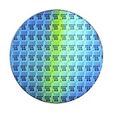
- Wafer Pattern May Vary from the Product Images. Great to be used as gift, display object, exhibition, educating demonstration, testing, decoration or your collection
- Beautiful microchip pattern structure made by the advanced copper technology
- 90~130nm minimum microchip feature Copper Characterization with TEOS or Black Diamond Low-k ILD on the single crystal silicon wafer
- The original value of un-polished wafer is above $500
- No guarantee for research and other applications
Castanares is best known for her leadership role at TSMC Arizona, where she has been closely associated with the company’s effort to bring advanced semiconductor manufacturing capacity to the Phoenix area. Her move to WaferTech connects two parts of TSMC’s U.S. footprint: the established Washington fab, which has operated for decades, and the newer Arizona expansion, which is central to TSMC’s future U.S. growth plans.
WaferTech gives Castanares a different kind of mandate from the Arizona project. Rather than leading a greenfield buildout, she will oversee a mature manufacturing site with an existing workforce, production base, customer commitments, supplier relationships, and operational culture. That makes the role less about launching a new fab from the ground up and more about sustaining performance, aligning the site with TSMC’s broader global manufacturing standards, and positioning WaferTech for relevance as U.S.-based semiconductor capacity becomes more strategically valuable.
What’s actually slowing this PC down?
Pick the symptom - the matching free tool is one click away.
The appointment also signals that TSMC wants continuity and stronger coordination across its American operations. WaferTech may not attract the same attention as the multibillion-dollar Arizona fabs, but it remains an part of TSMC’s U.S. presence. By naming a leader with recent experience in TSMC’s high-profile U.S. expansion, the company is reinforcing the idea that its American manufacturing network should operate as a connected platform rather than as isolated sites.
WaferTech’s Role in TSMC’s U.S. Manufacturing Footprint
WaferTech occupies a distinct place in TSMC’s American manufacturing story: it is not the company’s newest or most advanced U.S. fab, but it has been one of its longest-running physical anchors in the country. Based in Camas, Washington, WaferTech was established in the 1990s as a joint venture involving TSMC and other partners, giving the Taiwan-based foundry an early manufacturing presence in the United States well before the current wave of semiconductor reshoring incentives and national supply-chain planning.
The facility has historically focused on mature semiconductor process technologies rather than the leading-edge nodes associated with TSMC’s newest fabs in Taiwan and Arizona. That distinction matters. Mature-node capacity remains essential for a wide range of end markets, including automotive electronics, industrial controls, power management, consumer devices, communications equipment, and embedded systems. These chips may not always draw the same attention as advanced processors, but they are deeply embedded in everyday hardware and are often difficult to replace quickly when supply tightens.
How WaferTech complements TSMC’s U.S. presence
WaferTech gives TSMC an operating base with an existing U.S. workforce, established local supplier relationships, and experience running semiconductor production under American regulatory, environmental, and labor conditions. That operating history can be valuable as TSMC expands its U.S. footprint more aggressively through its Arizona investments. While Arizona is designed around advanced-node production for high-performance computing, artificial intelligence, mobile, and other demanding applications, WaferTech represents a different but still relevant layer of domestic manufacturing capacity.
- Geographic diversification: WaferTech adds a Pacific Northwest manufacturing site to TSMC’s U.S. map, separate from the company’s large-scale Arizona buildout.
- Mature-node production: The fab supports chip categories that remain critical for autos, industrial systems, and connected devices.
- Operational continuity: Its long-running U.S. manufacturing base gives TSMC institutional knowledge outside Taiwan.
- Customer support: A domestic facility can help certain customers seeking regional manufacturing options, qualification paths, or supply-chain resilience.
For customers, WaferTech’s value is tied less to headline-grabbing process leadership and more to reliability, continuity, and proximity. Companies that use mature or specialty processes often care about stable output, predictable qualifications, and long product life cycles. A fab such as WaferTech can support those needs by maintaining proven technologies and serving as part of a broader manufacturing network rather than as a standalone replacement for TSMC’s high-volume Taiwan operations.
Within TSMC’s wider U.S. footprint, WaferTech also serves as a reminder that American semiconductor manufacturing is not limited to cutting-edge chips. A resilient chip ecosystem requires a mix of advanced nodes, mature nodes, packaging, materials, equipment servicing, engineering support, and trained technicians. WaferTech’s role is therefore complementary: it helps broaden TSMC’s domestic base while the company’s larger Arizona projects aim to bring advanced manufacturing closer to major U.S. customers and strategic end markets.
Also popular on Amazon
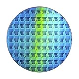
- Wafer Pattern May Vary from the Product Images. Great to be used as gift, display object, exhibition, educating demonstration, testing, decoration or your collection
- Beautiful microchip pattern structure made by the advanced copper technology
- 90~130nm minimum microchip feature Copper Characterization with TEOS or Black Diamond Low-k ILD on the single crystal silicon wafer
- The original value of un-polished wafer is above $500
- No guarantee for research and other applications
Why the Leadership Change Matters Now
TSMC’s decision to appoint a new president for WaferTech comes at a moment when U.S.-based semiconductor manufacturing is under closer scrutiny from customers, policymakers, and supply-chain planners. WaferTech, located in Camas, Washington, is not the centerpiece of TSMC’s newest American investment wave, but it remains an established operating site with a long production history, a local workforce, and existing customer commitments. A leadership change there can signal how TSMC intends to manage its mature U.S. assets while it builds much larger capacity elsewhere in the country.
The timing matters because TSMC is balancing two different manufacturing priorities in the United States. On one side, the company is investing heavily in advanced-node production in Arizona, where its fabs are intended to serve demand from major chip designers, high-performance computing customers, and artificial intelligence supply chains. On the other side, WaferTech represents an older but still strategically useful part of the company’s footprint, with established processes, supplier relationships, and operational know-how. New leadership can help align the Washington site with this broader U.S. plan rather than treating it as a standalone legacy operation.
Key areas affected by the transition
- Operational discipline: A new president can review manufacturing efficiency, equipment utilization, yield performance, and maintenance practices at a site that has been operating for decades.
- Workforce continuity: WaferTech depends on experienced engineering, technician, and production teams, making leadership stability central to retention and training.
- Customer confidence: Customers using mature process technologies value predictability, consistent quality, and clear communication during management transitions.
- U.S. coordination: The appointment may strengthen links between WaferTech, TSMC’s Arizona buildout, and the company’s broader North American customer support network.
The change also arrives during a period when semiconductor buyers are trying to reduce exposure to geographic bottlenecks. Even when a facility is not producing the most advanced chips, local capacity can matter for industrial, automotive, communications, and specialty applications that rely on stable mature-node supply. WaferTech’s role may therefore be less about competing with leading-edge fabs and more about supporting a diversified manufacturing base. Effective leadership can help the site maintain dependable output, manage costs, and adapt to customer needs as supply chains become more regionalized.
For TSMC, the appointment is also a governance signal. Running a U.S. fab involves labor-market constraints, environmental permitting, energy costs, local supplier coordination, and engagement with state and federal stakeholders. The president of WaferTech must operate within TSMC’s global manufacturing standards while responding to American operating conditions. If the new leader can improve coordination across these areas, WaferTech could become more valuable as a stable anchor in TSMC’s U.S. presence, complementing the company’s larger Arizona ambitions rather than being overshadowed by them.
How the Move Fits Into TSMC’s Broader U.S. Strategy
The leadership change at WaferTech sits within a much larger shift in TSMC’s manufacturing map. For decades, the company’s most advanced production has been concentrated in Taiwan, supported by a global network of design, customer support, and specialty manufacturing sites. In the United States, WaferTech has served as TSMC’s long-running operational base, giving the company experience with U.S. labor practices, environmental permitting, utility coordination, equipment maintenance, and customer requirements. Naming a new president for the joint venture helps align that mature site with a more ambitious American manufacturing agenda.
That agenda is centered on TSMC’s large investment in Arizona, where the company is building leading-edge wafer fabrication capacity aimed at serving major U.S. customers in high-performance computing, artificial intelligence, smartphones, automotive electronics, and defense-adjacent supply chains. While WaferTech in Washington is not the same type of project as the new Arizona fabs, it remains strategically relevant. It provides TSMC with an established U.S. operating platform at a time when the company is scaling hiring, supplier relationships, compliance systems, and manufacturing discipline across mulle American locations.
Windows Errors? Fix Them Before They Spread
Repair common Windows errors and clear accumulated junk for a smoother, more stable PC - no reinstall needed.Free scan · no reinstallCrashes, No Sound, or Screen Glitches?
Random freezes, missing sound and display glitches usually trace back to one bad driver. Find and replace yours safely.Free scan · under a minuteHow WaferTech complements Arizona
- Operational continuity: WaferTech gives TSMC a seasoned U.S. manufacturing organization while Arizona ramps newer facilities and teams.
- Workforce knowledge: The site offers practical experience in recruiting, training, retention, and plant management in the American semiconductor labor market.
- Supplier engagement: A long-standing U.S. fab helps strengthen relationships with materials, gases, chemicals, spare-parts, construction, and facilities-service providers.
- Customer reassurance: A refreshed leadership structure can signal that TSMC is not treating older U.S. assets as secondary while investing heavily in new ones.
The appointment also reflects the increasing importance of local execution. TSMC’s U.S. strategy depends not only on capital spending but also on the ability to run fabs with predictable yields, stable output, strong safety performance, and reliable delivery schedules. Semiconductor customers care about technology road maps, but they also care about whether a manufacturing partner can keep tools running, qualify processes on time, protect intellectual property, and respond quickly when demand changes. A president with a clear mandate at WaferTech can help tighten decision-making and improve coordination between local teams and TSMC’s global manufacturing organization.
Geopolitics adds another layer. U.S. policymakers and major chip buyers are pushing for more geographically distributed production after years of supply disruptions, pandemic-era shortages, shipping bottlenecks, and heightened concern over Taiwan Strait risk. TSMC’s American footprint is therefore part commercial strategy and part supply-chain resilience strategy. Strengthening WaferTech’s leadership supports that broader posture by reinforcing the company’s ability to operate credible manufacturing capacity on U.S. soil while its next-generation Arizona investments progress through construction, tool installation, qualification, and ramp-up.
Also popular on Amazon

- 5 x 5 inches, 0.67 ounces, 0.03 inches thick. Some wafers are marked with alignment marks.
- The pattern is produced by light diffraction, and its reflective appearance changes with the viewing angle.
- Silicon wafers are fragile—please handle with care.
- Circuit details can be examined under a microscope.
For TSMC, the move is less about replacing one site with another and more about building a connected U.S. manufacturing system. WaferTech can remain a useful anchor for domestic operations, even as Arizona becomes the focal point for advanced-node production. The new president’s role will be to keep the Washington operation competitive, dependable, and integrated with the company’s expanding American presence. If executed well, that could make TSMC’s U.S. strategy look less like a single megaproject and more like a durable regional manufacturing network.
Potential Impact on Operations, Customers, and Supply Chains
The appointment of a new WaferTech president is unlikely to change TSMC’s technology roadmap overnight, but it can shape how the Camas, Washington, fab performs inside the company’s U.S. manufacturing network. For operations, the most immediate effects are likely to be seen in execution: fab utilization, equipment uptime, workforce planning, supplier coordination, and the pace at which process improvements are implemented. A focused leadership team can help align WaferTech’s mature-node production with customer demand while keeping the site tightly connected to TSMC’s global manufacturing standards.
Recommended Free Tools
For customers, WaferTech’s value lies less in headline-grabbing leading-edge capacity and more in dependable U.S.-based production for chips used across industrial, automotive, communications, consumer, and specialty applications. Mature and specialty processes remain a large part of semiconductor demand, especially for power management, sensors, connectivity components, microcontrollers, and mixed-signal devices. If the new leadership improves cycle times, yield stability, or scheduling discipline, customers could see more predictable deliveries from a domestic fab that complements TSMC’s larger overseas production base.
Operational areas that could see renewed focus
- Manufacturing efficiency: tighter control of tool availability, wafer starts, cycle time, and output consistency.
- Workforce development: recruitment, retention, training, and knowledge transfer across engineering, maintenance, and operations teams.
- Supplier coordination: closer management of materials, spare parts, gases, chemicals, and maintenance services used by the fab.
- Customer responsiveness: better alignment between production planning and demand from North American customers.
- Site integration: stronger links between WaferTech, TSMC’s corporate manufacturing organization, and its expanding Arizona operations.
The leadership change also has supply-chain implications. Semiconductor buyers have spent the past several years reassessing geographic concentration, inventory strategy, and long lead times. WaferTech cannot replace TSMC’s much larger fabs in Taiwan, and it is not positioned as the centerpiece of the company’s advanced-node expansion in the United States. Even so, a stable U.S. wafer source gives customers another layer of flexibility, particularly for products that do not require the most advanced manufacturing nodes but still need proven quality systems and reliable output.
Within TSMC’s broader U.S. footprint, WaferTech may serve as a practical bridge between established domestic production and the company’s newer, more capital-intensive investments in Arizona. The Camas facility already has an operating workforce, local supplier relationships, and experience running commercial production in the United States. Under new leadership, those assets could be used more deliberately to support operational learning, vendor development, and customer engagement across TSMC’s American presence.
For the wider semiconductor ecosystem, the effect will depend on execution. If WaferTech improves output predictability and maintains strong process control, it can strengthen confidence among customers seeking resilient sourcing options. If it also helps deepen domestic supplier relationships, the benefits could extend beyond a single fab to the services, materials, and equipment networks that support U.S. chip manufacturing. The appointment therefore matters not as a standalone personnel move, but as part of TSMC’s effort to make its American manufacturing base more coordinated, dependable, and commercially useful.
What to Watch Next for WaferTech and TSMC in the U.S.
With a new president in place at WaferTech, the next phase will be measured less by the title change itself and more by what follows on the factory floor, in customer engagements, and across TSMC’s U.S. manufacturing network. WaferTech’s Camas, Washington site is a mature asset, so near-term signals are likely to involve execution: equipment utilization, process stability, workforce retention, and the degree to which the facility is aligned with TSMC’s larger American expansion centered in Arizona.
One area to watch is whether WaferTech receives new investment aimed at modernization, specialty capacity, or operational integration with other TSMC sites. The facility has historically supported production on established process technologies rather than the most advanced nodes. That role can still be valuable, especially for customers that need reliable supply for industrial, automotive, communications, and consumer applications. If TSMC uses WaferTech to strengthen output in mature or specialty processes, the site could become a more visible part of the company’s U.S. supply-chain strategy.
Also popular on Amazon

- Genuine Silicon Wafer: crafted from high-purity silicon, this 12 inch silicon wafer features a precision double-side polished surface, delivering exceptional smoothness and mirror-like reflectivity on both sides, fitting well with tech decor needs; Please note: wafer pattern may vary from the product images
- Genuine Uncut Ic Silicon Wafer: this is a genuine uncut IC silicon wafer, not a replica or model; It preserves the original circular wafer form applied in semiconductor manufacturing, allowing you to experience real chip substrate material up close
- 12 Inch Large Size Versatile Display: with a full 12 inch diameter, this wafer provides a striking visual presence compared to smaller 6 or 8 inch wafers; Its larger size enhances the natural light interference patterns, creating subtle rainbow reflections under different lighting, ideal for desk display, office decor, exhibitions, or as a centerpiece for tech-inspired spaces; Silicon crystals are very fragile, please handle them as gently as possible
- Practical Stem Education Tool: a valuable teaching tool for STEM education, this semiconductor substrate helps illustrate how integrated circuits are manufactured; Great for classrooms, labs, or personal learning, it allows students to better understand wafer structure, fabrication processes, and the foundation of modern electronics in a tangible way
- Tech-inspired Gift: combining science and art, this silicon wafer makes a unique gift for engineers, programmers, students, and tech lovers, suitable for various gifting occasions without being overly decorative
Signals that could show the direction of the new leadership
- Capital spending at the Camas site: Announcements related to tools, facilities, cleanroom upgrades, or process improvements would suggest a broader mandate than routine management succession.
- Hiring and workforce programs: Expanded recruiting, training partnerships, or retention initiatives would indicate preparation for higher operational demands.
- Customer commitments: New or expanded supply agreements tied to U.S.-based production would show whether customers see WaferTech as part of their domestic sourcing plans.
- Coordination with Arizona fabs: Shared suppliers, engineering practices, or talent pipelines could reveal how TSMC is connecting its U.S. manufacturing assets.
- Product mix changes: Any shift toward higher-value specialty technologies could affect WaferTech’s long-term strategic relevance.
The leadership transition also comes as semiconductor customers are reassessing geographic risk. Many chip buyers are not simply asking where the most advanced wafers are made; they are also reviewing where supporting components, legacy-node devices, and specialty chips can be sourced. For those customers, WaferTech’s established U.S. presence may carry added weight if TSMC can demonstrate consistent delivery, predictable cycle times, and strong quality controls under its new leadership.
Another factor is how U.S. policy and incentives continue to shape manufacturing decisions. TSMC’s Arizona investments have drawn the most attention because of their scale and advanced-node ambitions, but a durable U.S. footprint often depends on more than one flagship project. WaferTech could support that footprint by offering operational experience, an existing supplier base, and a workforce familiar with semiconductor production in the United States. The new president’s ability to connect those strengths with TSMC’s broader goals will be a practical test of the appointment.
In the coming quarters, the clearest indicators will be operational rather than symbolic. Watch for whether WaferTech becomes more integrated into TSMC’s public U.S. strategy, whether the company highlights the site in customer discussions, and whether investments point to a larger role for mature-node and specialty manufacturing. If those signs emerge, the appointment will look like part of a wider effort to deepen TSMC’s American manufacturing base, not merely a change in local leadership.
Frequently Asked Questions
Who is the new president of WaferTech?
TSMC named a new president to lead WaferTech, its U.S.-based wafer manufacturing joint venture in Camas, Washington. The appointment puts a dedicated executive in charge of a facility that remains an part of TSMC’s long-running American manufacturing presence.
What does WaferTech do for TSMC in the United States?
WaferTech operates as a semiconductor manufacturing facility and has served as one of TSMC’s earliest production footholds in the U.S. While it is smaller and older than TSMC’s new Arizona fabs, it gives the company local operating experience, a trained workforce, and established relationships with U.S. suppliers and customers.
How does this leadership change affect TSMC’s U.S. expansion plans?
The move signals that TSMC is continuing to manage its existing U.S. assets alongside its much larger investment in Arizona. A new leader at WaferTech could help align the site’s operations, staffing, and customer support with TSMC’s broader American manufacturing strategy.
Do these 3 things before closing this tab:
1Fix the driver behind crashes, sound loss and screen glitches2Repair Windows errors before they cause bigger problems3Scan for outdated or missing drivers - takes under a minuteWill customers see any immediate changes from the WaferTech appointment?
Most customers should not expect sudden changes in product availability or qualification processes solely because of the leadership change. The more likely near-term effects are operational adjustments, closer coordination with TSMC’s U.S. teams, and potential improvements in responsiveness for customers that rely on domestic manufacturing support.
What should people watch next for WaferTech and TSMC in the U.S.?
Key developments include whether WaferTech receives new investment, equipment upgrades, expanded hiring, or a more defined role alongside the Arizona fabs. Readers should also watch how TSMC balances mature-node production, advanced-node expansion, workforce development, and supply-chain localization across its U.S. operations.
Bottom Line
TSMC’s appointment of a new president at WaferTech signals continued attention to the company’s long-running U.S. manufacturing footprint at a time when domestic chip production is under intense scrutiny. While WaferTech is smaller than TSMC’s major Arizona buildout, leadership stability there still matters for operational execution, customer support, and workforce continuity.
The next step is to watch how the new leadership aligns WaferTech with TSMC’s broader U.S. strategy, from capacity planning and process support to supply chain resilience. For customers and industry partners, the change reinforces that TSMC’s American presence is not limited to new fabs—it also depends on improving and integrating existing assets.
Quick wins for a faster PC:
Fix the driver behind crashes, sound loss and screen glitchesFind Drivers →Clear out junk files and repair common Windows errorsFree Scan →
