Recommended Free Tools
Some links on this page are affiliate links: if you buy through them we may earn a commission, at no extra cost to you.
Choose an AI-chip foundry by total program risk and delivered system performance, not by the smallest process-node number. Start with your workload, throughput and latency targets, power envelope, SRAM and I/O needs, die size, chiplet plan, HBM interface, package thermal limit, production volume and launch geography. Then make each candidate prove process PPA, PDK and IP maturity, package feasibility, yield learning, capacity and ramp commitments on your design.
A leading node can still lose if its HBM package is unavailable, its design kit is immature, its test flow is congested or it cannot reserve wafers when demand rises. Treat the foundry, package, assembly, test and commercial contract as one decision.

As an Amazon Associate I earn from qualifying purchases.
The Tool Desk
Outbyte PC Repair FREERepair Windows errors before they cause bigger problemsFix Now →Outbyte Driver Updater FREEFix the driver behind crashes, sound loss and screen glitchesFind Drivers →What should you freeze before contacting a foundry?
Foundries can only give a meaningful answer when the chip and system requirements are specific. Create a one-page baseline that every candidate receives under NDA.
- Workload: list model types, batch sizes, sparsity assumptions, precision formats and target inference or training throughput.
- Latency and power: set service-level latency, sustained and peak power, voltage rails and cooling method.
- Memory: define HBM generation and stack count, external memory interfaces, on-die SRAM capacity and required bandwidth.
- Physical design: estimate die area, reticle exposure, I/O count, SerDes speeds, analog blocks and chiplet partition.
- Package: specify 2.5D or 3D architecture, interposer or bridge approach, package outline, thermal resistance and known-good-die strategy.
- Business case: provide engineering-lot quantity, annual wafer demand, acceptable die cost, launch date and expected geographic demand.
- Compliance: identify automotive, industrial, export-control, data-residency or secure-design requirements.
This baseline prevents a common mistake: comparing a foundry’s headline transistor density with a different company’s estimate of complete-system performance.
#1 Best Overall

- [Ultra-Lightweight Ear Buds Designed for Small Ears] Each earbud weighs only 3.7g and features a compact, ergonomic in-ear design made especially for small ears. Secure, low-profile, and comfortable for workouts, all-day wear or overnight sleeping.The ultra-slim profile sits flush in your ear with no hard edges poking or rubbing, so you can even sleep on your side without discomfort.
- [Immersive Stereo Sound with TOZO OrigX Technology] TOZO OrigX tuning delivers clear vocals, balanced mids, and natural stereo sound for music, podcasts, and videos.
- [Long Battery Life for Daily Use] Get up to 7 hours of playtime on a single charge, with up to 32 hours total using the charging case—ideal for workdays, commuting, and extended listening sessions.
- [Bluetooth 5.3 & Stable Connection] Bluetooth 5.3 provides fast pairing, stable wireless performance, and reduced dropouts as you move around home or office.
- [Deep Bass with Clear Vocals] High-performance drivers produce punchy bass while keeping vocals clean and detailed for everyday listening.
Which process node is best for an AI accelerator?
The best node is the one that meets your PPA, SRAM, I/O, analog and reliability requirements with a production-ready PDK and libraries. A newer node is useful only when its density, frequency or efficiency gains outweigh higher mask cost, design effort, package constraints and ramp risk.
Compare delivered PPA, not marketing density
Request benchmark results using your operator mix, memory traffic, clock targets and voltage range. Ask for SRAM compiler options, bit-cell variants, leakage data, high-voltage devices, analog support and design rules. An accelerator dominated by SRAM, HBM links or high-speed SerDes may gain less from a logic shrink than a headline node comparison suggests.
Do these 3 things before closing this tab:
1Clear out junk files and repair common Windows errors2Scan for outdated or missing drivers - takes under a minute3Repair Windows errors before they cause bigger problemsCheck voltage, reliability and specialty options
AI systems combine dense digital logic with power delivery, clocking, analog monitoring and high-speed I/O. Confirm operating-voltage ranges, electromigration rules, electrostatic-discharge options, process monitors and qualification data. If the product has a long service life or regulated deployment, require the quality system and reliability evidence that applies to the exact process variant.
Ask what is actually in production
Separate a published roadmap from a qualified process. The RFQ should identify the PDK release, design-rule revision, library qualification status, current wafer-start location and the date at which your exact option can enter volume production. Require change-control terms so a late process or library revision does not silently invalidate timing, power or layout work.
Why is advanced packaging part of foundry selection?
For many AI accelerators, HBM integration, interposer or bridge capacity, thermal design and test throughput determine the launch schedule more than transistor density. Select wafer, package, assembly and test capabilities as a single manufacturing flow.
Map the complete package stack
Obtain a package feasibility study covering die-to-die links, interposer dimensions, microbumps, HBM placement, power-delivery network, warpage, thermal interface materials and package-level test. Ask which steps are performed by the foundry, an affiliated operation or an external OSAT, and who owns yield data across those handoffs.
Validate HBM and chiplet supply
HBM stacks and advanced substrates can have different lead times from wafers. Ask for committed monthly package starts, substrate sources, HBM qualification status, known-good-die handling and a plan for failed stacks. A wafer allocation without matching package and memory capacity is not a production allocation.
Rank #2

- 【IP68 Waterproof Multifunctinal Smart Watch】Torjalph fitness activity tracker smart watch is IP68 waterproof technology ,you can wear it when swimming,handwashing,it's rain-proof which means that you perform multiple exercise modes outside without worrying about sweat or rain corroding your fitness smart watch,and this watch equipped with a 230 mAh large capacity battery magnetic charging ,and this sports activity tracker watch can be used 5-7 days If fully charged.
- 【Larger 1.83'' Full Screen Watch & Multi-dial Selection】1.83 inch full HD color touch screen smart watch for men / women provides excellent 240*284 resolution image quality ,This Bluetooth smart watch offers a better touch experience and remarkable immersion and ,more than 200 watch faces for you to choose from App"Da Fit ", you can change the dial style according to your mood to wear keeping the world on your wrist
- 【Accurate Activity Tracker Smart Watch 】sports watch activity tracker uses sweat and dust resistant breathable silicone strap, our Fitness Tracker Smart Watch for Android iOS Phones supports 12 sports modes,walking,running,bicycle,swimming,badminton,basketball,football,rope skipping. This bluetooth calls smart watch for men women is lightweight and stylish, bringing more convenient and relaxing sports experience while also providing more protection.
- 【Your 24 Hour Personal Daily Health Monitor】Fitness watch for women men full touch screen IP67 waterproof bluetooth smartwatch for Android iOS Phones with heart rate blood pressure monitor multifunction Andriod smart watch with steps counter sleep monitor sports fitness watch, monitoring blood oxygen saturation allows you to understand your physical condition in real time to track fitness progress ,to know your health status in time.
- 【More Functions Bluetooth Call Smart Watch】This fitness activity smart watch full screen for iPhone and Android phones includes a bunch of new features including:The bluetooth smart watch can hang up the phone, receive and display WhatsAPP /Text /Facebook /Twitter /Messenger reminder.Support sedentary reminder, alarm clock, stopwatch, timer,weather information,music control, remote camera control compatible with Android 5.0 and above or iOS 9.0 and above smartphones.
Measure thermal and test limits early
Require thermal simulations at the planned power, not at a generic chip rating. Confirm burn-in, system-level test, probe-card availability, test-time assumptions and throughput at your volume. Package and test bottlenecks can raise usable-die cost even when wafer yield is strong.
Which foundries should an AI-chip team evaluate?
TSMC, Samsung Foundry and Intel Foundry are credible starting points, but none is automatically the right choice. Their public descriptions show capability and ecosystem breadth; your NDA evaluation must establish availability, yield, package capacity and commercial terms for the target program.
| Foundry | Public positioning and evidence | Questions to resolve for your program |
|---|---|---|
| TSMC | Its 2024 annual report describes a full range of advanced and specialty processes, advanced mask technology, TSMC 3DFabric advanced silicon stacking and packaging, manufacturing productivity and ecosystem support. TSMC reported 12,682 products, 305 distinct technologies and 534 customers in 2025. Its 2024 figures included 12.9 million 12-inch-equivalent wafer shipments, 69% of wafer revenue from 7nm-and-beyond technologies, 288 process technologies, 11,878 products and 522 customers. Four 12-inch GIGAFAB facilities exceeded 12.74 million 12-inch wafers of combined capacity in 2024. | Can your startup obtain wafer starts and advanced-package slots in the required quarter? Which site will run wafers and package the product, what are the fallback sites, and what commercial and geographic terms apply? Treat the scale figures as indicators, not a guarantee of allocation. |
| Intel Foundry | Announced in February 2024 as a systems-foundry model for the AI era, Intel Foundry presents an expanded process roadmap including Intel 14A, specialized nodes and Intel Foundry Advanced System Assembly and Test (ASAT). Intel said Synopsys, Cadence, Siemens and Ansys had validated tools, design flows and IP for Intel 18A. Its fact sheet describes a full-stack offering spanning IP, EDA, process nodes, advanced packaging and ASAT, with support for ARM, RISC-V, x86 and custom ASIC architectures. | Verify the exact node’s production date, yield history, customer references, package rules and capacity for your launch window. Clarify how a systems-level engagement affects design support, test ownership, supply-chain geography and migration if the schedule changes. |
| Samsung Foundry | Samsung describes a dedicated design platform covering libraries, PDKs, design methodology, IP, design support, packaging and cloud services. Its SAFE ecosystem links IP, EDA, cloud, DSP and OSAT partners. The MDI Alliance offers 2.5D and 3D heterogeneous-integration packaging as a one-stop service. | Request production references for the selected node and package, current PDK and IP revisions, geographic options, package/test capacity at your volume and the commercial model for engineering and ramp lots. |
Public customer counts, wafer shipments and roadmap statements are useful scale signals, but they do not reveal your queue position, design-specific yield or package availability. A confidential RFQ and technical review are required.
How do PDK, IP and EDA support affect first-silicon risk?
Design enablement often determines schedule more than a nominal transistor advantage. A mature PDK, silicon-proven IP and a reference signoff flow reduce the chance that your first tape-out fails for reasons unrelated to architecture.
Inspect the PDK release and change history
Ask for release dates, known issues, design-rule waivers, extraction decks, reliability decks and a list of changes between revisions. Confirm that the PDK supports the exact SRAM, I/O, SerDes, HBM, PCIe and DDR options in your specification rather than a nearby process variant.
Demand evidence for critical IP
For each third-party or foundry IP block, record process qualification, silicon revisions, performance corners, error-correction features, licensing scope and support response times. TSMC’s Open Innovation Platform is described as using silicon-verified, production-proven and quality-assessed IP and libraries to lower design barriers and improve first-time silicon success. Ask for comparable evidence from every candidate.
Review the complete EDA flow
Check synthesis, place-and-route, extraction, timing, power integrity, formal verification, physical verification, DFT and package co-design. Intel reported that Synopsys, Cadence, Siemens and Ansys validated tools, flows and IP for Intel 18A; still verify which tool versions, decks and support engineers are available to your project. A validated tool flow is not the same as a completed design using your blocks.
Rank #3
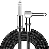
- [Low Noise High Fidelity] New bee guitar cord with 22AWG oxygen-free-copper center conductors provides enhanced signal transfer, the PVC insulation material and the high-density stranded copper double shield provide noise rejection for quiet operation
- [Ideal for Choice] New bee 1/4 straight and right angle metal connectors, ensures a secure connection in any instrument, pedal, or amp jack. L shape great fro on stage guitar stands
- [Wide Compatible] Suitable for mixer, power amplifier, microphone, effector, decoder, equalizer, electoronic organ, electric guitar, electric bass and other electronic equipments. Widely used in the installation of smart home, karaoke speaker, professional stage audio, etc
- [Easy Disassemble] Making incidental repairs quick and easy! Very nice, flexible cable
- [Dont Hesite to Order] 24 hours customer services and professional technology team are standing by
Price engineering support explicitly
Include application-engineer coverage, office hours, escalation paths, training, cloud access and on-site debug in the evaluation. Record response-time commitments and which issues are covered by the foundry fee versus a paid professional-service agreement.
How should you compare yield, capacity and ramp commitments?
Yield and capacity are contractual risks, not assumptions to make from a foundry’s reputation. Ask for measurable gates and remedies before committing the design.
Use a yield-learning plan
- Define defect-density targets and the statistical confidence required at each wafer milestone.
- Set qualification gates for parametric yield, functional yield, burn-in and package yield.
- Specify how failing wafers, dies and packages will be analyzed and how data will be shared.
- Document the known-good-die strategy for chiplets and HBM assemblies.
- Model usable-die cost at pilot, qualification and volume yields instead of using a single mature-yield assumption.
Reserve the whole manufacturing chain
Your capacity request should cover wafer starts, reticles, package assembly, substrates, HBM or other memory, probe, final test and burn-in. Ask whether reservations are firm, cancellable or take-or-pay; identify minimum volumes, lead times and expedite charges; and name fallback sites for wafers, packaging and test.
Plan for geographic disruption
Map the origin of wafers, reticles, substrates, gases, HBM, packaging and test. Require disaster-recovery procedures, export-control screening and a qualification path for a second site. A geographic alternative that has never run your design is not an immediate substitute, so budget time for requalification.
What should an AI-chip foundry RFQ include?
Public sources do not provide comparable foundry pricing. Send the same technical baseline and request a line-item quote so wafer price does not hide the real program cost.
| RFQ category | Request these terms | Decision use |
|---|---|---|
| Wafer and masks | Engineering wafers, production wafer price, reticles, mask/NRE charges, probe and metrology fees, lead times and validity period. | Builds a realistic tape-out and volume cost. |
| IP and EDA | License fees, royalties, minimum commitments, renewal rules, cloud or server charges and support scope for every required block and tool. | Reveals enablement cost that is absent from wafer quotes. |
| Package and test | Interposer or bridge, substrate, HBM integration, assembly, burn-in, final test, test development, probe cards, package NRE and per-unit pricing. | Exposes the package and test bottleneck. |
| Capacity reservation | Wafer-start allocation, package/test slots, ramp schedule, minimum volumes, cancellation rights, expedite fees and fallback locations. | Converts an informal forecast into supply protection. |
| Quality and change control | Qualification standards, traceability, audit rights, process-change notice, security controls, confidentiality and liability for nonconforming material. | Protects regulated products and design data. |
| Roadmap and migration | Committed production date, customer-qualification status, successor-node plan, porting assistance and requalification cost. | Separates available capacity from roadmap slides. |
Compare total risk-adjusted cost: design effort, schedule reserve, mask and engineering lots, expected usable dies, package/test, inventory, expedite exposure and the cost of a respin. A lower wafer quote can be more expensive if it carries immature IP or uncertain packaging.
Can a startup obtain advanced-node wafers and CoWoS-like packaging?
Startups can request access, but access is governed by capacity, technical readiness, volume, credit and the foundry’s customer-selection process. There is no public guarantee that an advanced node or an advanced package will be available to a new company at a desired date.
Rank #4

- Digital Family Calendar: BSIMB digital calendar wall touch screen puts an end to your chaotic life. Designed for busy families, the digital calendar keeps you organised and in step with your family. Assign different colours and tasks to each family member to make family scheduling easier and more intuitive.
- Easy Setup and Auto-Sync: Plug in, connect to WLAN and auto-syn your electric calendar in minutes. Digital wall calendar compatible with Google calendar, iCloud calendar, Outlook calendar, Cozi calendar and Yahoo calendar. Add events directly on the device or through the ecalendar app. Electronic calendar stays current whether you're at work or traveling—no manual updates needed.
- All-In-One Home Assistant: Smart calendar builds habits and encourage independence with personalised chores. Display daily meal plan to reduce the daily ‘What's for dinner?’ stress. To-do lists keep track of everything you want. Turning chores into valuable achievements with stars and rewards, making life easier and more enjoyable.
- Manage Anytime Anywhere: BSIMB electronic calendar for family stay connected with the powerful ecalendar app. Access and manage your digital wall calendar anytime, anywhere with free features like stars & rewards, photo screensaver, chore charts, meals plans, to-do lists etc. Electronic planner paid features like Magic Import tailor advanced tools for users with special needs.
- Stay in Touch with Loved Ones: Share photos or videos from your phone to electronic wall calendar with app, instantly update your life moment, and keep in touch with your family, especially those who are far away; you can also surprise your smart calendar digital wall by sending him a wish card; it's also great for keeping tech-illiterate elders in touch with the youngsters.
Make the program easy to qualify
- Prepare the workload, package, volume and launch specification before the introductory meeting.
- Bring an experienced design house, IP vendor or system partner if your team lacks advanced-node tape-out history.
- Sign the NDA and request the current PDK, package design kit, reference flows, IP catalog and support model.
- Offer a staged commitment: feasibility study, shuttle or engineering lot, qualification lot and volume ramp.
- Provide credible financing, forecast discipline and a purchase-order path for wafers, packages and test.
For CoWoS-like 2.5D integration, ask specifically about interposer or bridge capacity, HBM allocation, substrate lead time, thermal qualification, assembly yield and test throughput. If any of those is constrained, a nominal wafer reservation will not produce finished accelerators.
Quick wins for a faster PC:
Repair Windows errors before they cause bigger problemsFix Now →Fix the driver behind crashes, sound loss and screen glitchesFind Drivers →What is the step-by-step foundry selection process?
- Freeze the system specification. Record performance, latency, power, memory bandwidth, SRAM, die area, chiplet partition, package thermal limit, annual volume and launch geography.
- Shortlist two or three candidates. Eliminate processes that cannot meet voltage, I/O, SRAM, package or reliability requirements before requesting detailed quotes.
- Exchange NDA data. Obtain PDK maturity, IP availability, reference flows, yield history, package stack, engineering coverage and capacity plans.
- Run equivalent design studies. Use the same architecture assumptions and, where practical, shuttle silicon to compare PPA, design effort, schedule and risk-adjusted cost.
- Conduct package co-design. Close HBM, interposer, thermal, substrate, assembly and test feasibility before final node selection.
- Negotiate one integrated contract. Cover wafers, masks/NRE, engineering lots, package/test, capacity reservation, quality, change control, confidentiality and contingency sites together.
- Set stage gates. Tie payments and commitments to PDK release, IP qualification, tape-out readiness, first silicon, package qualification, yield milestones and volume ramp.
- Keep a fallback. Maintain a second-source, alternate-package or redesign plan when the economics justify the extra engineering, and identify the exact work needed to requalify it.
What mistakes most often derail foundry decisions?
Choosing the smallest node by default
A density label does not account for SRAM efficiency, analog availability, I/O, package bandwidth or reliability. Correct this by comparing complete accelerator benchmarks and physical-design estimates.
Buying wafers without securing packages
Advanced packaging, substrates, HBM and test may have separate queues. Correct this by obtaining written capacity and lead-time commitments for every step from wafer probe through final test.
Assuming ecosystem claims equal project readiness
A broad IP or EDA alliance can still leave your exact SerDes, HBM controller or signoff deck unqualified. Correct this by listing every required block and recording its process-specific qualification evidence.
Comparing wafer prices alone
Mask fees, engineering lots, IP, package NRE, test development, minimum volumes and expedite charges can dominate early cost. Correct this with a total-cost model based on usable packaged dies.
Treating allocation as a handshake
Forecasts do not protect capacity during an AI demand spike. Correct this by negotiating reservation terms, cancellation rules, escalation contacts and fallback locations before tape-out.
Leaving portability until after tape-out
Standard cells, IP, timing, power delivery, package rules and yield learning are tightly coupled to a process. Correct this by estimating the requalification work and preserving an alternate path while architecture and package decisions are still flexible.
How can you score the final candidates?
Use a weighted scorecard that reflects your product’s bottleneck rather than a generic ranking. A suggested structure is:
| Category | Evidence to score | Typical weighting question |
|---|---|---|
| System PPA | Equivalent design-study throughput, latency, power and memory bandwidth. | Does this process improve delivered performance enough to matter? |
| Enablement | PDK revision, IP qualification, EDA decks, application support and known issues. | Can the team reach tape-out without unplanned rework? |
| Package execution | HBM, interposer or 3D feasibility, thermal results, assembly and test capacity. | Can finished systems ship, not merely wafers? |
| Yield and ramp | Defect targets, qualification gates, yield-learning data and time-to-volume plan. | What usable-die cost and launch date are credible? |
| Supply resilience | Reserved wafer and package slots, site diversity, materials and disaster plans. | What happens if demand or a site disruption changes the plan? |
| Economics and contract | Total risk-adjusted cost, minimums, cancellation, change control and liability. | Are savings real after NRE, package and respin exposure? |
Require written evidence for every high-weight score. If a candidate cannot disclose a number, mark it as an unresolved risk and price the contingency instead of awarding an optimistic score.
What’s actually slowing this PC down?
Pick the symptom - the matching free tool is one click away.
What is the practical decision rule?
Select the foundry that can demonstrate the best probability of shipping your complete, thermally viable AI system on schedule at an acceptable usable-die cost. That may be the largest pure-play ecosystem, a systems-oriented provider with integrated assembly and test, or an alternative with a better-fitting PDK, package and geographic plan. Make the choice only after equivalent design evidence, package feasibility, capacity commitments and contractual protections are in hand.
Frequently Asked Questions
How early should an AI-chip company approach a foundry?
Begin during architecture, before the node and package are frozen. Early engagement lets the team check PDK access, HBM and substrate lead times, package rules, engineering-lot timing and capacity reservations while those choices can still change.
Does a foundry guarantee yield for a new AI design?
No. Foundries can provide process-level targets and qualification data, but customer-specific yield depends on layout, IP, memory, package and test. Contractual milestones and a shared yield-learning plan are more useful than a generic mature-yield claim.
Is a second source practical for an advanced AI accelerator?
Only with deliberate planning. Standard cells, libraries, IP, physical constraints, package rules and yield learning are not directly portable, so a second source usually requires a requalification or redesign budget and an early architectural decision.
PC Slower Than It Used to Be?
A free scan shows the junk files, broken settings and background clutter dragging Windows down - then fixes them in one click.Free scan · Windows 10 & 11Crashes, No Sound, or Screen Glitches?
Random freezes, missing sound and display glitches usually trace back to one bad driver. Find and replace yours safely.Free scan · under a minuteWhat information should a startup keep confidential in an RFQ?
Share enough workload, package and volume detail for a credible feasibility study under NDA, while controlling model data, architectural diagrams, unreleased benchmarks, customer information and security-sensitive implementation details. Define ownership and permitted use of design files and yield data in the agreement.
How do package constraints change the chip architecture?
HBM count, interposer area, die-to-die links, power delivery and thermal limits can force changes to die size, chiplet boundaries, memory partitioning and clock targets. Co-designing the package before tape-out avoids discovering that a theoretically fast die cannot be assembled or cooled at volume.
Quick Recap
Product prices and availability are accurate as of the date/time indicated and are subject to change. Any price and availability information displayed on Amazon at the time of purchase will apply.

