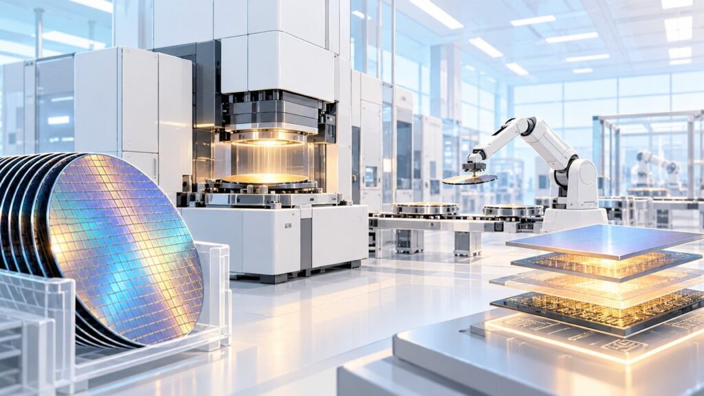
A semiconductor fabrication facility, or fab, is a factory where integrated circuits are built layer by layer on polished silicon wafers. Hundreds or thousands of tightly controlled operations—deposition, lithography, etching, doping, cleaning, measurement and inspection—are repeated for each layer. A wafer can spend several weeks in processing, and ASML says the broader path from design to mass production can take up to four months. The finished wafer is diced into individual dies, packaged and tested.
What a semiconductor fab actually does
A fab does not print a complete chip in one pass. It creates a vertical stack of microscopic structures on a shared silicon substrate. Each wafer carries many repeated copies of a circuit, called dies, so hundreds or thousands of chips can be processed in parallel. The exact count depends on wafer diameter and die size.

As an Amazon Associate I earn from qualifying purchases.
The Semiconductor Industry Association divides the value chain into three broad activities:
Free tools Windows power users keep installed
One-click scans. No signup required.
- Design: engineers define the circuit architecture, layouts and manufacturing rules.
- Front-end wafer fabrication: the fab forms transistors and the metal interconnect that links them.
- Assembly and testing: the wafer is cut into dies, each die is packaged, connected and electrically tested.
“Fab” describes the physical plant. “Foundry” describes a business relationship in which a manufacturer makes chips designed by other companies. A company can therefore operate a fab without being a foundry, and a foundry can run many fabs for different customers.
#1 Best Overall

- [Ultra-Lightweight Ear Buds Designed for Small Ears] Each earbud weighs only 3.7g and features a compact, ergonomic in-ear design made especially for small ears. Secure, low-profile, and comfortable for workouts, all-day wear or overnight sleeping.The ultra-slim profile sits flush in your ear with no hard edges poking or rubbing, so you can even sleep on your side without discomfort.
- [Immersive Stereo Sound with TOZO OrigX Technology] TOZO OrigX tuning delivers clear vocals, balanced mids, and natural stereo sound for music, podcasts, and videos.
- [Long Battery Life for Daily Use] Get up to 7 hours of playtime on a single charge, with up to 32 hours total using the charging case—ideal for workdays, commuting, and extended listening sessions.
- [Bluetooth 5.3 & Stable Connection] Bluetooth 5.3 provides fast pairing, stable wireless performance, and reduced dropouts as you move around home or office.
- [Deep Bass with Clear Vocals] High-performance drivers produce punchy bass while keeping vocals clean and detailed for everyday listening.
From refined silicon to a usable wafer
Growing a single-crystal ingot
Chipmaking starts with silicon refined to extremely high purity. The silicon is melted and formed into a single-crystal ingot. A single crystal matters because an orderly atomic lattice gives engineers predictable electrical behavior and allows transistors to be made consistently across the wafer.
Slicing and polishing
A diamond saw slices the ingot into thin discs. The discs are ground, chemically treated and polished until the surface is exceptionally flat and smooth. The result is a mirror-like wafer with controlled thickness and a surface suitable for depositing and patterning films.
Common wafer diameters
Modern and mature processes use several standard diameters. Larger wafers offer more area for dies in one processing run, but they require compatible equipment, recipes and handling systems.
| Wafer format | Nominal diameter | Typical role |
|---|---|---|
| 300 mm | 12 inches | High-volume production for many advanced and mainstream processes |
| 200 mm | 8 inches | Large installed base for mature logic, analog, power, sensors and other products |
| 150 mm | 6 inches | Older or specialized production lines |
These diameters are not interchangeable by simply changing a setting. A fab needs wafer-handling robots, process chambers, metrology and statistical controls designed for the selected format. After processing, the wafer is sawn into individual dies.
The repeated wafer-processing loop
Every patterned layer follows a related sequence. Recipes differ by material and device type, but the core loop is deposition, resist coating, exposure, development, etch or implantation, stripping, cleaning and measurement.
1. Deposition adds a thin film
Deposition places a controlled film on the wafer. Depending on the layer, the film may conduct electricity, insulate adjacent conductors or act as a semiconductor. Chemical-vapor, physical-vapor and atomic-layer techniques are examples of ways fabs build films, although the exact method depends on the material and required thickness.
2. Photoresist coating creates a temporary stencil
The wafer is coated with a light-sensitive material called photoresist. It is spun at high speed so the resist spreads into a uniform film. Thickness and uniformity matter because they affect how light exposes the pattern and how the subsequent development and etch behave.
Quick wins for a faster PC:
Scan for outdated or missing drivers - takes under a minuteDriver Scan →Clear out junk files and repair common Windows errorsFree Scan →Fix the driver behind crashes, sound loss and screen glitchesFind Drivers →3. Lithography exposes the pattern
A reticle, often called a mask, carries a circuit pattern larger than the feature that will remain on the wafer. In ASML’s description, “A lithography (more formally known as ‘photolithography’) system is essentially a projection system.” Light passes through or reflects from the reticle, and precision optics reduce and focus the image onto the resist.
Rank #2

- 【IP68 Waterproof Multifunctinal Smart Watch】Torjalph fitness activity tracker smart watch is IP68 waterproof technology ,you can wear it when swimming,handwashing,it's rain-proof which means that you perform multiple exercise modes outside without worrying about sweat or rain corroding your fitness smart watch,and this watch equipped with a 230 mAh large capacity battery magnetic charging ,and this sports activity tracker watch can be used 5-7 days If fully charged.
- 【Larger 1.83'' Full Screen Watch & Multi-dial Selection】1.83 inch full HD color touch screen smart watch for men / women provides excellent 240*284 resolution image quality ,This Bluetooth smart watch offers a better touch experience and remarkable immersion and ,more than 200 watch faces for you to choose from App"Da Fit ", you can change the dial style according to your mood to wear keeping the world on your wrist
- 【Accurate Activity Tracker Smart Watch 】sports watch activity tracker uses sweat and dust resistant breathable silicone strap, our Fitness Tracker Smart Watch for Android iOS Phones supports 12 sports modes,walking,running,bicycle,swimming,badminton,basketball,football,rope skipping. This bluetooth calls smart watch for men women is lightweight and stylish, bringing more convenient and relaxing sports experience while also providing more protection.
- 【Your 24 Hour Personal Daily Health Monitor】Fitness watch for women men full touch screen IP67 waterproof bluetooth smartwatch for Android iOS Phones with heart rate blood pressure monitor multifunction Andriod smart watch with steps counter sleep monitor sports fitness watch, monitoring blood oxygen saturation allows you to understand your physical condition in real time to track fitness progress ,to know your health status in time.
- 【More Functions Bluetooth Call Smart Watch】This fitness activity smart watch full screen for iPhone and Android phones includes a bunch of new features including:The bluetooth smart watch can hang up the phone, receive and display WhatsAPP /Text /Facebook /Twitter /Messenger reminder.Support sedentary reminder, alarm clock, stopwatch, timer,weather information,music control, remote camera control compatible with Android 5.0 and above or iOS 9.0 and above smartphones.
4. Bake and development reveal openings
Heating steps stabilize the resist chemistry. A developer then dissolves selected regions, depending on whether the resist is positive or negative. The remaining resist protects some portions of the underlying film while openings expose other portions for removal or modification.
5. Etching transfers the pattern into the film
Etch tools remove material through the resist openings. Dry etching uses reactive plasma and can provide highly directional profiles. Wet etching uses liquid chemicals and can be selective for particular materials. The goal is a three-dimensional feature with the intended width, depth and sidewall shape.
6. Ion implantation tunes silicon
Ion implantation accelerates charged dopant ions into selected silicon regions. Dopants change the local electrical conductivity and help form transistor source, drain and other structures. A later heat treatment repairs crystal damage and activates the dopants.
7. Resist stripping and cleaning prepare the next operation
Once the pattern has served its purpose, the remaining resist is removed. Wet chemistries, plasma cleaning and ultrapure water rinses remove residues and particles. Incomplete cleaning can contaminate later layers, so cleaning is a manufacturing step rather than housekeeping.
8. Metrology and inspection close the feedback loop
Optical and electron-beam systems measure critical dimensions, film thickness, overlay alignment and defects. Process-control software compares results with targets. Engineers adjust recipes, exposure settings, chamber conditions or maintenance schedules when measurements drift.
How lithography makes tiny features
Lithography determines where later etch, deposition or implantation occurs. The reticle pattern is intentionally larger than the final printed feature; the projection optics shrink it, focus it and align it with patterns already present on the wafer.
EUV and DUV have different jobs
Extreme ultraviolet (EUV) systems are used for the smallest critical layers in leading-edge processes. Deep ultraviolet (DUV) systems handle larger or less critical layers and remain important across advanced and mature production. A single chip can therefore use both tool classes rather than relying on one exposure technology for every layer.
Recommended Free Tools
Computational lithography corrects predictable errors
At nanometer dimensions, diffraction, focus variation, resist chemistry and etch behavior distort the intended image. Computational lithography uses manufacturing models, tool data and test-wafer measurements to pre-correct the reticle or exposure recipe. The correction improves pattern fidelity and makes a process more manufacturable, which can raise yield.
Rank #3
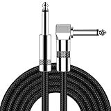
- [Low Noise High Fidelity] New bee guitar cord with 22AWG oxygen-free-copper center conductors provides enhanced signal transfer, the PVC insulation material and the high-density stranded copper double shield provide noise rejection for quiet operation
- [Ideal for Choice] New bee 1/4 straight and right angle metal connectors, ensures a secure connection in any instrument, pedal, or amp jack. L shape great fro on stage guitar stands
- [Wide Compatible] Suitable for mixer, power amplifier, microphone, effector, decoder, equalizer, electoronic organ, electric guitar, electric bass and other electronic equipments. Widely used in the installation of smart home, karaoke speaker, professional stage audio, etc
- [Easy Disassemble] Making incidental repairs quick and easy! Very nice, flexible cable
- [Dont Hesite to Order] 24 hours customer services and professional technology team are standing by
Why a chip needs many aligned layers
Transistors occupy only part of a finished integrated circuit. Additional layers provide contacts, local wiring, vias and increasingly thick metal interconnects that connect billions of devices. ASML says modern chips may contain up to 100 layers, each requiring nanometer-scale overlay alignment.
Overlay is the registration of one layer to the previous one. A tiny shift can create an open circuit, a short or a transistor with the wrong electrical characteristics. Because errors can accumulate over many levels, fabs measure alignment repeatedly and feed the results back into scanners, etch tools and process recipes.
Why fab cleanrooms are so controlled
A particle that is invisible to a person can be large enough to destroy a die or interrupt a narrow metal line. ASML describes fab cleanrooms as about 10,000 times cleaner than outside air, with many facilities operating at ISO Class 1 conditions.
The Tool Desk
Outbyte PC Repair FREERepair Windows errors before they cause bigger problemsFix Now →Outbyte Driver Updater FREEFix the driver behind crashes, sound loss and screen glitchesFind Drivers →Cleanliness is only one part of the control system. Fabs also regulate:
- Temperature and humidity: resist chemistry, film growth and tool calibration are sensitive to environmental changes.
- Vibration: floor movement can blur a lithography exposure or disturb measurement.
- Chemical and gas purity: trace contaminants can alter film properties or dope a surface unintentionally.
- Airflow and filtration: filtered, recirculated air limits particles around open wafers.
- Wafer handling: sealed carriers and automated transport reduce human contact and contamination.
- Equipment calibration: exposure dose, pressure, temperature, gas flow and alignment must remain within narrow windows.
These controls are expensive, but a small excursion can affect many wafers before it is detected. Preventing the excursion is usually cheaper than sorting or scrapping a large batch.
What yield means and why it drives economics
Intel defines yield as “the percentage of usable die that are produced on a processed wafer.” Yield is therefore measured at the die level, not simply as the percentage of wafers that completed processing.
Common causes of bad dies
- Particles, scratches or other contamination
- Defective or non-uniform deposited films
- Layer-to-layer overlay errors
- Line-edge roughness and imperfect resist patterns
- Etch profiles that are too deep, shallow, wide or narrow
- Unstable temperature, pressure, chemistry or exposure dose
- Tool wear, calibration drift or a chamber fault
Inspection identifies where defects occur, while metrology shows whether dimensions and materials remain within specification. Statistical process control tracks variation over time. If a measurement begins trending toward a limit, engineers can intervene before a large number of dies fail.
PC Slower Than It Used to Be?
A free scan shows the junk files, broken settings and background clutter dragging Windows down - then fixes them in one click.Free scan · Windows 10 & 11Crashes, No Sound, or Screen Glitches?
Random freezes, missing sound and display glitches usually trace back to one bad driver. Find and replace yours safely.Free scan · under a minuteWhy wafer diameter alone does not determine cost
A 300 mm wafer has more area than a 200 mm wafer, but useful output also depends on die area, defect density and process maturity. Larger dies fit fewer times across a wafer and have a higher chance of intersecting a defect. A mature process with low defect density can outperform a newer process that has more nominal wafer area but lower usable yield. Throughput, equipment cost, cycle time and packaging capacity also affect economics.
Rank #4

- Digital Family Calendar: BSIMB digital calendar wall touch screen puts an end to your chaotic life. Designed for busy families, the digital calendar keeps you organised and in step with your family. Assign different colours and tasks to each family member to make family scheduling easier and more intuitive.
- Easy Setup and Auto-Sync: Plug in, connect to WLAN and auto-syn your electric calendar in minutes. Digital wall calendar compatible with Google calendar, iCloud calendar, Outlook calendar, Cozi calendar and Yahoo calendar. Add events directly on the device or through the ecalendar app. Electronic calendar stays current whether you're at work or traveling—no manual updates needed.
- All-In-One Home Assistant: Smart calendar builds habits and encourage independence with personalised chores. Display daily meal plan to reduce the daily ‘What's for dinner?’ stress. To-do lists keep track of everything you want. Turning chores into valuable achievements with stars and rewards, making life easier and more enjoyable.
- Manage Anytime Anywhere: BSIMB electronic calendar for family stay connected with the powerful ecalendar app. Access and manage your digital wall calendar anytime, anywhere with free features like stars & rewards, photo screensaver, chore charts, meals plans, to-do lists etc. Electronic planner paid features like Magic Import tailor advanced tools for users with special needs.
- Stay in Touch with Loved Ones: Share photos or videos from your phone to electronic wall calendar with app, instantly update your life moment, and keep in touch with your family, especially those who are far away; you can also surprise your smart calendar digital wall by sending him a wish card; it's also great for keeping tech-illiterate elders in touch with the youngsters.
Yield is not one universal percentage. It varies by product, die size, process maturity, factory conditions and the definition of a shippable die. A yield figure without those qualifications is not a meaningful comparison.
Front end, back end and packaging
Front-end wafer fabrication
Front-end processing creates the transistor structures and the interconnect layers on the wafer. The repeated loop may run hundreds of times, with cleaning and measurement between critical operations. Wafers remain in carriers while automated systems move them among deposition, lithography, etch, implant and inspection tools.
Dicing and assembly
When all wafer layers are complete, a diamond saw or other singulation process separates the wafer into dies. Each usable die is attached to a package substrate or lead frame. Electrical connections are formed with methods such as wire bonding or flip-chip interconnects, depending on the product.
What’s actually slowing this PC down?
Pick the symptom - the matching free tool is one click away.
Testing and thermal design
Finished packages are electrically tested, marked and inspected. The package protects the die, routes signals and supplies power. It also transfers heat to a spreader, heat sink or the system board. For high-performance processors and other demanding devices, package construction is part of the electrical and thermal design—not merely a protective container.
Independent reader supportYour contribution helps us test, update, and keep practical guides available for everyone.Who operates a fab?
| Business model | What the company does | Typical relationship |
|---|---|---|
| Integrated device manufacturer (IDM) | Designs and manufactures chips, often in its own fabs | One company controls both product design and wafer production for at least part of its portfolio |
| Pure-play foundry | Manufactures chips designed by customers | Customers provide circuit designs and manufacturing requirements; the foundry runs the process |
| Fabless semiconductor company | Focuses on architecture, design and product software while outsourcing wafer fabrication | Uses one or more foundries and later assembly and test partners |
Intel and Samsung are examples of IDMs. TSMC, GlobalFoundries and UMC are examples of pure-play foundries. Many processor and graphics companies are fabless. These categories can overlap in practice: an IDM may outsource some products, and a fabless company may own test or packaging operations.
How to compare two fabs or process technologies
“Node” names are not literal measurements of one transistor dimension. Intel describes a process node as a recipe and ingredient set for fabrication. A useful comparison should therefore examine several axes:
- Feature size and layer criticality: which dimensions are most demanding and on which layers?
- EUV and DUV capability: which exposure technologies are available, and for what layers?
- Wafer diameter: 300, 200 or 150 mm capacity affects area and equipment economics.
- Process maturity: newer recipes may offer smaller features but need time to stabilize.
- Defect density and yield: usable dies matter more than nominal wafer area.
- Throughput and cycle time: how quickly can the fab process wafers without sacrificing control?
- Packaging technology: advanced packages can affect bandwidth, power delivery and thermal performance.
- Business model: an IDM and a customer-facing foundry optimize capacity and design support differently.
Many fabs do not target leading-edge logic. Mature-node facilities remain important for analog, power management, sensors, automotive electronics, industrial controls and memory. A larger feature size can be the right choice when the product values voltage handling, reliability, cost or long qualification cycles over maximum transistor density.
Do these 3 things before closing this tab:
1Scan for outdated or missing drivers - takes under a minute2Clear out junk files and repair common Windows errors3Fix the driver behind crashes, sound loss and screen glitchesHow long the journey takes
ASML says the path from design to mass production can take up to four months. Intel describes wafers passing through thousands of processing steps over several weeks before packaging. The exact schedule depends on the product, number of layers, queue time, rework, inspection holds and factory capacity.
A simplified flow looks like this:
- Designers finish the circuit layout and manufacturing checks.
- The fab prepares wafers, reticles, recipes and process-control plans.
- Wafers run through repeated deposition, lithography, etch, implant, clean and measurement steps.
- Inspection data are reviewed; wafers may be held, reworked or rejected when results exceed limits.
- Completed wafers are electrically probed to classify good and bad die locations.
- Usable dies are singulated, packaged and tested again as finished parts.
A beginner’s mental model: one transistor layer becoming a chip
Imagine a blank polished wafer. A conductive or insulating film is deposited, resist is coated and a reticle image exposes selected areas. Development opens windows, etch transfers the pattern, and cleaning removes the temporary resist. Ion implantation then changes selected silicon regions so they can function as transistor source and drain areas. Measurement checks whether the dimensions and alignment match the recipe.
The fab repeats that logic for contacts, gates and multiple wiring levels. Each new pattern must line up with the structures below it. After dozens of cycles—and potentially up to 100 total layers—the wafer contains many complete circuits. Dicing separates them, and packaging turns each surviving die into a component that can connect to a circuit board or another package.
Common misconceptions
“Lithography writes the whole chip at once”
It does not. The scanner projects one reticle field at a time and steps across the wafer. Different reticles and process loops create different layers.
“A smaller node automatically means a better chip”
Not for every product. Performance, power, reliability, analog behavior, high-voltage capability, cost, yield and packaging all matter. A mature process can be the better engineering choice for a sensor or power device.
“A bigger wafer guarantees lower cost”
Only if the fab has compatible equipment, high throughput and good yield. Die size, defect density, process stability and packaging capacity determine how many sellable parts result.
“The package is just a box”
The package carries signals and power, removes heat and protects the die. Its electrical and thermal characteristics can limit the performance of the finished chip.
Why semiconductor fabs matter
Fabs turn an abstract circuit design into millions or billions of repeatable physical devices. Their advantage comes from control: control of contamination, film thickness, pattern placement, materials, temperature, equipment and feedback. In 2021, ASML reported semiconductor shipments of 1.15 trillion units—about 145 chips for every person—illustrating the scale of the industry. At that volume, a small yield improvement or a tiny reduction in cycle time can have a major economic effect.
The essential idea is simple: deposit a film, pattern it with lithography, modify or remove selected regions, clean the wafer, measure the result and repeat. The difficulty lies in repeating that sequence across an entire wafer, across many layers, with nanometer alignment and enough consistency that most dies work.
Quick Recap
Product prices and availability are accurate as of the date/time indicated and are subject to change. Any price and availability information displayed on Amazon at the time of purchase will apply.

