TSMC leads Samsung in advanced chip manufacturing because it has been more consistent at turning process research into high-volume, high-yield production while operating at much larger foundry scale. Its pure-play business model reduces customer conflict, its broad fabless customer base keeps leading-edge lines learning and loaded, and its advanced-packaging portfolio extends the advantage beyond the transistor.
Samsung remains a serious technology competitor. It has delivered important FinFET, EUV and gate-all-around (GAA) milestones, and it offers advanced packaging. The documented gap is execution at scale: Samsung’s FY2025 materials identify stabilizing advanced-node mass-production yields, improving utilization and attracting more customers as priorities.

As an Amazon Associate I earn from qualifying purchases.
What “leading” means in advanced manufacturing
A smaller nanometer number or an earlier announcement does not by itself make a foundry the leader. Customers need a process that is qualified, produces enough good dies per wafer, runs at predictable volume and connects to packaging, design tools and supply-chain services. The useful comparison is therefore the time from process development to reliable high-volume manufacturing, not the date of a technology reveal.
“Yield” is the share of manufactured dies that meet specification. A process with a lower defect rate produces more saleable chips from each wafer, lowering effective cost and making capacity usable. Public company sources do not provide a directly comparable, audited yield table for every TSMC and Samsung advanced node, so precise percentage claims about one company’s yield advantage cannot be established from official disclosures.
#1 Best Overall

- [Ultra-Lightweight Ear Buds Designed for Small Ears] Each earbud weighs only 3.7g and features a compact, ergonomic in-ear design made especially for small ears. Secure, low-profile, and comfortable for workouts, all-day wear or overnight sleeping.The ultra-slim profile sits flush in your ear with no hard edges poking or rubbing, so you can even sleep on your side without discomfort.
- [Immersive Stereo Sound with TOZO OrigX Technology] TOZO OrigX tuning delivers clear vocals, balanced mids, and natural stereo sound for music, podcasts, and videos.
- [Long Battery Life for Daily Use] Get up to 7 hours of playtime on a single charge, with up to 32 hours total using the charging case—ideal for workdays, commuting, and extended listening sessions.
- [Bluetooth 5.3 & Stable Connection] Bluetooth 5.3 provides fast pairing, stable wireless performance, and reduced dropouts as you move around home or office.
- [Deep Bass with Clear Vocals] High-performance drivers produce punchy bass while keeping vocals clean and detailed for everyday listening.
Company-reported indicators of TSMC’s scale
| Measure | TSMC figure | How to read it |
|---|---|---|
| Advanced-process share of wafer revenue | 69% in 2024 | Company-reported share from 7nm and smaller processes; it indicates how much of TSMC’s wafer business is concentrated in advanced nodes. |
| Advanced-process share of wafer revenue | 74% in 2025 | Company-reported share from 7nm and smaller processes; this is a revenue mix measure, not a yield percentage. |
| Foundry 2.0 share | 34% in 2024 | TSMC’s company-reported share of its expanded Foundry 2.0 market definition, which includes logic manufacturing, packaging, testing, mask-making and related activities. |
| Annual manufacturing capacity | More than 17 million 12-inch-equivalent wafers in 2025 | Company-reported total annual capacity. It is a 12-inch-equivalent measure, not a count of only the newest-node wafers. |
| 2nm production status | High-volume manufacturing in the fourth quarter of 2025, with good yield | TSMC’s reported milestone concerns volume production and yield, not merely a laboratory demonstration. |
These numbers are reported by TSMC in its 2024 and 2025 materials. They show scale and mix, but they do not constitute an independent, side-by-side audit against Samsung.
Process maturity is the first source of the lead
From a node announcement to a usable process
An advanced node requires a long sequence: transistor and interconnect development, design-rule definition, electronic-design-automation (EDA) enablement, test-chip learning, customer design qualification, yield improvement and finally repeatable volume output. A company can announce a node before all of those steps are complete. The decisive question for a chip designer is when wafers can be ordered in predictable quantities with acceptable defect levels.
TSMC’s reported 2nm high-volume manufacturing in the fourth quarter of 2025, with good yield, is evidence of that conversion from development to production. The wording matters: high-volume manufacturing and yield are operational milestones, whereas a first transistor demonstration is not.
Samsung’s documented execution challenge
Samsung Foundry has real leading-edge achievements, including the first 14nm FinFET process, 7nm EUV process and 3nm GAA process. Its roadmap includes 2nm SF2 variants and a 1.4nm GAA generation, alongside AI-assisted yield-improvement work and turnkey heterogeneous packaging.
Rank #2

- 【IP68 Waterproof Multifunctinal Smart Watch】Torjalph fitness activity tracker smart watch is IP68 waterproof technology ,you can wear it when swimming,handwashing,it's rain-proof which means that you perform multiple exercise modes outside without worrying about sweat or rain corroding your fitness smart watch,and this watch equipped with a 230 mAh large capacity battery magnetic charging ,and this sports activity tracker watch can be used 5-7 days If fully charged.
- 【Larger 1.83'' Full Screen Watch & Multi-dial Selection】1.83 inch full HD color touch screen smart watch for men / women provides excellent 240*284 resolution image quality ,This Bluetooth smart watch offers a better touch experience and remarkable immersion and ,more than 200 watch faces for you to choose from App"Da Fit ", you can change the dial style according to your mood to wear keeping the world on your wrist
- 【Accurate Activity Tracker Smart Watch 】sports watch activity tracker uses sweat and dust resistant breathable silicone strap, our Fitness Tracker Smart Watch for Android iOS Phones supports 12 sports modes,walking,running,bicycle,swimming,badminton,basketball,football,rope skipping. This bluetooth calls smart watch for men women is lightweight and stylish, bringing more convenient and relaxing sports experience while also providing more protection.
- 【Your 24 Hour Personal Daily Health Monitor】Fitness watch for women men full touch screen IP67 waterproof bluetooth smartwatch for Android iOS Phones with heart rate blood pressure monitor multifunction Andriod smart watch with steps counter sleep monitor sports fitness watch, monitoring blood oxygen saturation allows you to understand your physical condition in real time to track fitness progress ,to know your health status in time.
- 【More Functions Bluetooth Call Smart Watch】This fitness activity smart watch full screen for iPhone and Android phones includes a bunch of new features including:The bluetooth smart watch can hang up the phone, receive and display WhatsAPP /Text /Facebook /Twitter /Messenger reminder.Support sedentary reminder, alarm clock, stopwatch, timer,weather information,music control, remote camera control compatible with Android 5.0 and above or iOS 9.0 and above smartphones.
However, Samsung’s FY2025 disclosures describe stabilizing advanced-node mass-production yields and improving fab utilization as active priorities. That does not mean the technology is nonfunctional; it means the commercial challenge is making output sufficiently consistent and filling the available capacity with enough customer products. TSMC’s advantage is therefore best described as a more repeatable ramp, not a monopoly on transistor innovation.
Yield turns wafer capacity into competitive capacity
Why good dies per wafer matter
Wafer starts are only the beginning of economics. A wafer contains many potential dies, but defects, parametric failures and packaging tests remove some of them. Higher yield means more conforming dies from the same wafer start, so a customer can obtain more chips without adding as many wafers. Better yield also makes delivery schedules and unit costs easier to forecast.
Yield learning accelerates when a process runs many wafers across many products. Defects are found in different layouts and operating conditions; engineers can then correct design rules, equipment settings and process steps. A large, diverse production base gives a foundry more opportunities to learn than a lightly loaded line.
The Tool Desk
Outbyte PC Repair FREEClear out junk files and repair common Windows errorsFree Scan →Outbyte Driver Updater FREEFix the driver behind crashes, sound loss and screen glitchesFind Drivers →What the public data can and cannot prove
Official disclosures establish that TSMC reported good-yield 2nm high-volume manufacturing and that Samsung is working to stabilize advanced-node mass-production yields. They do not publish a complete, node-by-node series using identical test methods. Rumored yield percentages should therefore not be treated as a verified TSMC–Samsung comparison.
Rank #3
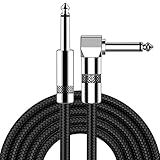
- [Low Noise High Fidelity] New bee guitar cord with 22AWG oxygen-free-copper center conductors provides enhanced signal transfer, the PVC insulation material and the high-density stranded copper double shield provide noise rejection for quiet operation
- [Ideal for Choice] New bee 1/4 straight and right angle metal connectors, ensures a secure connection in any instrument, pedal, or amp jack. L shape great fro on stage guitar stands
- [Wide Compatible] Suitable for mixer, power amplifier, microphone, effector, decoder, equalizer, electoronic organ, electric guitar, electric bass and other electronic equipments. Widely used in the installation of smart home, karaoke speaker, professional stage audio, etc
- [Easy Disassemble] Making incidental repairs quick and easy! Very nice, flexible cable
- [Dont Hesite to Order] 24 hours customer services and professional technology team are standing by
Scale creates a learning and investment loop
Capacity and fixed-cost absorption
TSMC’s more than 17 million 12-inch-equivalent wafers of annual capacity in 2025 spread expensive tools, facilities and engineering resources across a very large output base. Its broad process portfolio allows the company to reuse manufacturing know-how and infrastructure while serving products at different performance, power and cost points.
TSMC also reported a 34% share of the Foundry 2.0 industry in 2024. Because Foundry 2.0 includes packaging, testing, mask-making and related activities in addition to logic wafer fabrication, the figure should not be read as a pure wafer-foundry share. It nevertheless illustrates the breadth of the ecosystem TSMC is counting when it describes its position.
The reinforcing loop
- More customers create more wafer starts. Different chip designs expose the process to varied patterns and operating conditions.
- More starts generate more defect data. Engineers can identify systematic problems sooner and refine recipes and design rules.
- Improved yield lowers effective cost and raises confidence. Customers are more willing to qualify the process for large products.
- Higher demand supports further investment. Revenue and utilization help finance the next node and additional capacity.
This loop does not guarantee success at every generation, but it makes a mature, heavily used platform harder for a smaller or less-utilized competitor to displace.
Quick wins for a faster PC:
Clear out junk files and repair common Windows errorsFree Scan →Scan for outdated or missing drivers - takes under a minuteDriver Scan →Pure-play neutrality attracts fabless customers
TSMC’s business model is another structural advantage. In its 2024 Annual Report, the company states: “By choosing not to design, manufacture or market any semiconductor products under its own name, the Company ensures that it never competes with its customers.” That is the core pure-play promise: TSMC sells manufacturing services rather than branded chips that could compete with a customer’s product.
Rank #4

- Digital Family Calendar: BSIMB digital calendar wall touch screen puts an end to your chaotic life. Designed for busy families, the digital calendar keeps you organised and in step with your family. Assign different colours and tasks to each family member to make family scheduling easier and more intuitive.
- Easy Setup and Auto-Sync: Plug in, connect to WLAN and auto-syn your electric calendar in minutes. Digital wall calendar compatible with Google calendar, iCloud calendar, Outlook calendar, Cozi calendar and Yahoo calendar. Add events directly on the device or through the ecalendar app. Electronic calendar stays current whether you're at work or traveling—no manual updates needed.
- All-In-One Home Assistant: Smart calendar builds habits and encourage independence with personalised chores. Display daily meal plan to reduce the daily ‘What's for dinner?’ stress. To-do lists keep track of everything you want. Turning chores into valuable achievements with stars and rewards, making life easier and more enjoyable.
- Manage Anytime Anywhere: BSIMB electronic calendar for family stay connected with the powerful ecalendar app. Access and manage your digital wall calendar anytime, anywhere with free features like stars & rewards, photo screensaver, chore charts, meals plans, to-do lists etc. Electronic planner paid features like Magic Import tailor advanced tools for users with special needs.
- Stay in Touch with Loved Ones: Share photos or videos from your phone to electronic wall calendar with app, instantly update your life moment, and keep in touch with your family, especially those who are far away; you can also surprise your smart calendar digital wall by sending him a wish card; it's also great for keeping tech-illiterate elders in touch with the youngsters.
Why the model reduces customer risk
- Fewer strategic conflicts: a fabless chip designer does not have to share sensitive production information with a foundry that markets a competing chip line.
- Portfolio flexibility: TSMC can serve multiple customers in the same broad market without favoring its own device business.
- Shared ecosystem investment: process design kits, EDA support and packaging options can be developed for a wide customer population.
Samsung operates a major branded electronics and semiconductor business as well as its foundry operation. That integrated structure brings engineering depth and internal demand, but some external customers may evaluate the additional competitive relationship when choosing a manufacturing partner. It is a potential conflict-of-interest consideration, not proof that Samsung mishandles customer information.
Independent reader supportYour contribution helps us test, update, and keep practical guides available for everyone.Advanced packaging extends the contest beyond the wafer
TSMC’s integrated options
Modern accelerators and other complex systems increasingly combine multiple dies rather than relying on one very large monolithic die. TSMC combines leading-edge logic with packaging and 3D-integration technologies such as CoWoS, InFO and SoIC. These cover different approaches to placing dies side by side, stacking them or integrating them with advanced interconnects.
For a customer, access to a qualified package can be as important as access to the transistor node. A fast die that cannot be assembled with sufficient bandwidth, thermal performance or production volume is not a complete product. Coordinating wafer process and package development can shorten qualification and reduce integration risk.
Recommended Free Tools
Samsung’s packaging capability
Samsung also offers 2.5D and 3D packaging through its MDI Alliance and promotes turnkey heterogeneous integration. Its packaging technology is therefore a genuine competitive strength. The difference is not whether Samsung has advanced packaging; it is whether the complete process-and-package combination is available at the volume, yield and customer breadth required for a particular design.
Customer breadth and ecosystem effects
A broad fabless customer base helps a foundry keep advanced factories productive between individual product cycles. It also encourages third-party design houses, EDA vendors, intellectual-property providers and packaging partners to support the process. Once those tools and services are widely deployed, a new customer can start a design with less risk and fewer missing components.
TSMC’s reported strong AI-related demand and record 2024–2025 performance fit this ecosystem effect, but no single customer explains the lead. The durable advantage comes from many customers, repeated qualifications and the resulting utilization and learning.
TSMC and Samsung compared on the factors customers actually buy
| Decision factor | TSMC | Samsung Foundry |
|---|---|---|
| Time to reliable high-volume production | Reported 2nm high-volume manufacturing in Q4 2025 with good yield. | FY2025 materials emphasize stabilizing advanced-node mass-production yields; a complete comparable timeline is not published. |
| Yield and usable dies | Good-yield 2nm production is reported, but no independently audited node-by-node series is provided. | Yield stabilization is an identified priority; no complete comparable series is provided. |
| Customer alignment | Pure-play model; the company says it does not design, manufacture or market products under its own name. | Foundry is part of a diversified semiconductor and electronics company, creating both internal engineering advantages and a potential competitive relationship for outside customers. |
| Manufacturing scale | More than 17 million 12-inch-equivalent wafers of annual capacity in 2025; 34% of the company’s 2024 Foundry 2.0 market definition. | Capacity figure comparable to TSMC’s disclosed measure is not stated in the cited FY2025 materials. |
| Process and transistor technology | Broad leading-node portfolio, including reported 2nm high-volume manufacturing. | Firsts in 14nm FinFET, 7nm EUV and 3nm GAA; developing 2nm SF2 variants and a 1.4nm GAA roadmap. |
| Advanced packaging | CoWoS, InFO, SoIC and other 3D-integration technologies. | 2.5D/3D packaging through the MDI Alliance and turnkey heterogeneous packaging. |
Samsung’s strengths should not be mistaken for a lack of capability
Samsung’s GAA work, EUV experience and packaging integration give customers a technically credible alternative. Its integrated company structure can support investment across memory, logic, packaging and systems, while its AI-assisted yield-improvement efforts target exactly the operational bottleneck identified in its FY2025 disclosures.
Free tools Windows power users keep installed
One-click scans. No signup required.
The issue is conversion and consistency. A roadmap, a first-of-kind process and a production-ready platform are different stages. Samsung must stabilize yields, raise utilization and win enough external designs for learning to compound. If it does, the competitive gap can narrow even without matching TSMC on every measure.
How to evaluate future claims about the gap
When a new node is announced, check these questions before declaring a winner:
- Is the claim a research demonstration, risk production or high-volume manufacturing?
- Does the company report yield or only a transistor milestone?
- Are customer products named as being qualified or in volume shipment?
- Is capacity stated in comparable wafer units, and is it total capacity or capacity at the new node?
- Does the offer include design enablement, testing and an advanced package?
- Are the two companies using equivalent node definitions? Nanometer labels are not standardized across foundries.
- Is the figure company-reported, independently audited or an unattributed estimate?
On the evidence available through 2025, TSMC leads because it repeatedly turns advanced process development into dependable volume, operates at exceptional scale, aligns naturally with fabless customers and links wafer manufacturing to advanced packaging. Samsung has many of the underlying technologies, but its own disclosures show that yield stabilization, utilization and customer expansion remain the steps needed to turn those technologies into a comparable, durable manufacturing platform.
Quick Recap
Product prices and availability are accurate as of the date/time indicated and are subject to change. Any price and availability information displayed on Amazon at the time of purchase will apply.

