Japan is the stronger choice for an advanced-node fab that needs an established semiconductor ecosystem and demonstrated strategic-project funding. India is the more straightforward option when the investment case depends on a published 50% central-support formula for a broad range of greenfield fabs, specialty devices and packaging plants. Neither country can be declared universally cheaper or more profitable from the available official material: comparable figures for electricity, water, land, labour, permitting time, taxes, yields and total cost of ownership are not published.
The practical answer therefore depends on the facility. A leading-edge logic or strategic memory project will find more execution evidence in Japan. A first domestic fab, compound-semiconductor plant, sensor line, photonics facility or ATMP/OSAT operation may find India’s percentage-based programme easier to map to a preliminary business case.

As an Amazon Associate I earn from qualifying purchases.
India and Japan use different subsidy models
The headline percentages and yen amounts answer different questions. India’s modified semiconductor programme states that the government will provide 50% of project cost on a pari-passu basis for all technology nodes for qualifying silicon fabs. The same programme offers 50% of capital expenditure for specified compound-semiconductor, silicon-photonics, sensor, discrete-semiconductor and ATMP/OSAT facilities. Japan’s support is generally negotiated project by project, with awards tied to named investments, technology objectives, production milestones and supply-security goals.
Quick wins for a faster PC:
Repair Windows errors before they cause bigger problemsFix Now →Scan for outdated or missing drivers - takes under a minuteDriver Scan →| Comparison point | India | Japan |
|---|---|---|
| Core subsidy design | Published 50% project-cost support for qualifying silicon fabs across technology nodes; 50% capex support for listed specialty and packaging facilities | Project-specific grants approved for strategic investments and linked to national technology and supply-security priorities |
| Programme scale cited in official material | Semicon India outlay of ₹76,000 crore | More than ¥10 trillion in public support for AI and semiconductors through fiscal 2030 |
| Examples of fab or memory awards | Broad formula rather than a single comparable award amount in the cited material | Up to ¥732 billion for JASM’s second fab; up to ¥150 billion for the Kioxia-Western Digital advanced 3D NAND investment |
| Advanced-logic support example | All technology nodes are within the published fab scope, subject to programme approval | Up to ¥590 billion in additional Rapidus support announced in April 2024 |
| Design incentive | Up to 50% of eligible product-design expenditure, capped at ₹15 crore per application, plus a 6% to 4% deployment incentive on net sales over five years, capped at ₹30 crore per application | The cited material does not provide a directly comparable national design-incentive formula |
A percentage is not automatically a larger economic benefit than a large negotiated grant. The value of India’s formula depends on the approved project-cost base, eligible-cost definitions, disbursement schedule and the investor’s ability to finance the remaining share. Japan’s awards can be very large in absolute terms, but an applicant cannot assume that the same percentage or amount will be available to a different project.
#1 Best Overall

- [Ultra-Lightweight Ear Buds Designed for Small Ears] Each earbud weighs only 3.7g and features a compact, ergonomic in-ear design made especially for small ears. Secure, low-profile, and comfortable for workouts, all-day wear or overnight sleeping.The ultra-slim profile sits flush in your ear with no hard edges poking or rubbing, so you can even sleep on your side without discomfort.
- [Immersive Stereo Sound with TOZO OrigX Technology] TOZO OrigX tuning delivers clear vocals, balanced mids, and natural stereo sound for music, podcasts, and videos.
- [Long Battery Life for Daily Use] Get up to 7 hours of playtime on a single charge, with up to 32 hours total using the charging case—ideal for workdays, commuting, and extended listening sessions.
- [Bluetooth 5.3 & Stable Connection] Bluetooth 5.3 provides fast pairing, stable wireless performance, and reduced dropouts as you move around home or office.
- [Deep Bass with Clear Vocals] High-performance drivers produce punchy bass while keeping vocals clean and detailed for everyday listening.
What India offers a chip manufacturer
Silicon fabs across technology nodes
The modified programme’s most important feature is its breadth. It expressly covers “all technology nodes” under the scheme for setting up semiconductor fabs in India and sets fiscal support at 50% of project cost on a pari-passu basis. That wording gives a greenfield applicant a clear starting point for modelling central support whether the planned line targets mature, specialty or more advanced silicon processes. It does not mean every proposal receives an automatic payment: the project still has to satisfy the scheme, pass approval and document eligible expenditure.
Specialty semiconductors and packaging
India also publishes 50% capex support for compound semiconductors, silicon photonics, sensors, discrete semiconductors and ATMP/OSAT facilities. This matters for companies whose first Indian operation is not a conventional front-end silicon fab. A packaging and test project, for example, can use the same headline share as a specialty-device facility, although the eligible-cost calculation and technical requirements will differ by category.
Programme envelope and institutional route
The Semicon India programme has a total outlay of ₹76,000 crore. Applications and programme information are handled through the central India Semiconductor Mission framework. The programme is intended to build domestic manufacturing and a supporting supply chain rather than only subsidise one isolated plant. India has also signed semiconductor-supply-chain cooperation arrangements, including with Japan, which can help structure cross-border technology and supply relationships; the existence of an agreement does not itself guarantee a grant or a site approval.
Design-linked support
India’s Design Linked Incentive is relevant when a manufacturing project is paired with local chip or system design. It can cover up to 50% of eligible product-design expenditure, subject to a cap of ₹15 crore per application. A separate deployment incentive pays between 6% and 4% of net sales over five years, with a cap of ₹30 crore per application. These limits make the instrument more material for early product development and commercialisation than for financing a large wafer-fab build.
Rank #2

- 【IP68 Waterproof Multifunctinal Smart Watch】Torjalph fitness activity tracker smart watch is IP68 waterproof technology ,you can wear it when swimming,handwashing,it's rain-proof which means that you perform multiple exercise modes outside without worrying about sweat or rain corroding your fitness smart watch,and this watch equipped with a 230 mAh large capacity battery magnetic charging ,and this sports activity tracker watch can be used 5-7 days If fully charged.
- 【Larger 1.83'' Full Screen Watch & Multi-dial Selection】1.83 inch full HD color touch screen smart watch for men / women provides excellent 240*284 resolution image quality ,This Bluetooth smart watch offers a better touch experience and remarkable immersion and ,more than 200 watch faces for you to choose from App"Da Fit ", you can change the dial style according to your mood to wear keeping the world on your wrist
- 【Accurate Activity Tracker Smart Watch 】sports watch activity tracker uses sweat and dust resistant breathable silicone strap, our Fitness Tracker Smart Watch for Android iOS Phones supports 12 sports modes,walking,running,bicycle,swimming,badminton,basketball,football,rope skipping. This bluetooth calls smart watch for men women is lightweight and stylish, bringing more convenient and relaxing sports experience while also providing more protection.
- 【Your 24 Hour Personal Daily Health Monitor】Fitness watch for women men full touch screen IP67 waterproof bluetooth smartwatch for Android iOS Phones with heart rate blood pressure monitor multifunction Andriod smart watch with steps counter sleep monitor sports fitness watch, monitoring blood oxygen saturation allows you to understand your physical condition in real time to track fitness progress ,to know your health status in time.
- 【More Functions Bluetooth Call Smart Watch】This fitness activity smart watch full screen for iPhone and Android phones includes a bunch of new features including:The bluetooth smart watch can hang up the phone, receive and display WhatsAPP /Text /Facebook /Twitter /Messenger reminder.Support sedentary reminder, alarm clock, stopwatch, timer,weather information,music control, remote camera control compatible with Android 5.0 and above or iOS 9.0 and above smartphones.
What Japan offers a chip manufacturer
Large, named project awards
Japan’s Ministry of Economy, Trade and Industry (METI) presents support as a portfolio of negotiated awards. Its official subsidy presentation lists up to ¥732 billion for JASM’s second fab and up to ¥150 billion for the Kioxia-Western Digital advanced 3D NAND investment. Those figures appear within a ¥1.699 trillion package shown in the presentation. The awards are tied to specific projects, so they demonstrate Japan’s willingness to fund large facilities but do not establish a universal subsidy rate for every applicant.
A national framework through fiscal 2030
METI’s AI and semiconductor framework states that Japan plans more than ¥10 trillion in public support through fiscal 2030. The stated objective is to induce more than ¥50 trillion in public-private investment and approximately ¥160 trillion in economic ripple effects over ten years. These are policy targets, not a guaranteed return for an individual fab. They indicate that semiconductor funding is being treated as a long-term industrial and economic-security programme rather than a one-off construction grant.
Rapidus and advanced logic
In April 2024, METI announced up to ¥590 billion in additional support for Rapidus: up to ¥536.5 billion for front-end processes and ¥53.5 billion for advanced back-end processes. In November 2025, METI selected Rapidus for support under the amended information-processing law and said it intended to invest ¥100 billion from the fiscal-2025 initial budget through the Information-technology Promotion Agency (IPA). The sequence of approvals is evidence of continuing public commitment to an advanced-logic capability, while the project-specific nature of the decisions means a new entrant must negotiate its own terms.
Do these 3 things before closing this tab:
1Repair Windows errors before they cause bigger problems2Fix the driver behind crashes, sound loss and screen glitches3Clear out junk files and repair common Windows errorsSupply-security orientation
Japan’s ministerial statements frame semiconductors as technology supporting digitalisation, decarbonisation and economic security. The cited awards span advanced logic, memory and related strategic capacity. Japan also has existing materials, equipment and device projects that can connect to a new fab. That depth can reduce the number of supply-chain relationships an investor must build from zero, although it does not remove the need to qualify suppliers, secure utilities and meet Japanese regulatory requirements.
Rank #3
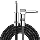
- [Low Noise High Fidelity] New bee guitar cord with 22AWG oxygen-free-copper center conductors provides enhanced signal transfer, the PVC insulation material and the high-density stranded copper double shield provide noise rejection for quiet operation
- [Ideal for Choice] New bee 1/4 straight and right angle metal connectors, ensures a secure connection in any instrument, pedal, or amp jack. L shape great fro on stage guitar stands
- [Wide Compatible] Suitable for mixer, power amplifier, microphone, effector, decoder, equalizer, electoronic organ, electric guitar, electric bass and other electronic equipments. Widely used in the installation of smart home, karaoke speaker, professional stage audio, etc
- [Easy Disassemble] Making incidental repairs quick and easy! Very nice, flexible cable
- [Dont Hesite to Order] 24 hours customer services and professional technology team are standing by
Which country gives the bigger semiconductor subsidy?
There is no honest single-number winner. India publishes a potentially very high share of an approved project’s cost, while Japan publishes very large absolute awards for selected projects. To compare them, an investor must put both offers into the same model:
- Define the same facility boundary: land, buildings, cleanroom, process tools, utilities, waste treatment, installation, validation and initial working capital.
- Separate eligible and ineligible expenditure under each country’s rules.
- Set the same production capacity, node, product mix and ramp schedule.
- Map when each payment arrives rather than treating an announced maximum as cash available on day one.
- Include any required private co-investment, local contributions, guarantees, technology-transfer conditions or supply-security commitments.
For a very large strategic project, Japan’s cited grants may exceed the nominal value of a smaller Indian project even though India’s percentage is higher. For a qualifying Indian project with a large approved cost base, the 50% formula can produce substantial support. The figures cannot be ranked without a project-level award decision and a common cost definition.
Technology fit: match the incentive to the factory
Leading-edge logic
Japan has the clearer execution record for advanced logic because the cited Rapidus decisions identify front-end and back-end support and are embedded in a national advanced-semiconductor strategy. India’s rules do not exclude advanced nodes—the published wording covers all technology nodes—but the official material cited here does not provide a comparable, funded advanced-node operating record or yield history. A leading-edge applicant should therefore treat India as a policy opportunity requiring deeper project diligence, not as an already proven equivalent.
The Tool Desk
Outbyte Driver Updater FREEScan for outdated or missing drivers - takes under a minuteDriver Scan →Outbyte PC Repair FREEClear out junk files and repair common Windows errorsFree Scan →Memory
Japan’s cited support for advanced 3D NAND gives memory investors a concrete project precedent. India’s broad fab and packaging categories may still accommodate memory-related manufacturing, but the material supplied does not identify an equivalent Indian memory award or operating benchmark.
Rank #4

- Digital Family Calendar: BSIMB digital calendar wall touch screen puts an end to your chaotic life. Designed for busy families, the digital calendar keeps you organised and in step with your family. Assign different colours and tasks to each family member to make family scheduling easier and more intuitive.
- Easy Setup and Auto-Sync: Plug in, connect to WLAN and auto-syn your electric calendar in minutes. Digital wall calendar compatible with Google calendar, iCloud calendar, Outlook calendar, Cozi calendar and Yahoo calendar. Add events directly on the device or through the ecalendar app. Electronic calendar stays current whether you're at work or traveling—no manual updates needed.
- All-In-One Home Assistant: Smart calendar builds habits and encourage independence with personalised chores. Display daily meal plan to reduce the daily ‘What's for dinner?’ stress. To-do lists keep track of everything you want. Turning chores into valuable achievements with stars and rewards, making life easier and more enjoyable.
- Manage Anytime Anywhere: BSIMB electronic calendar for family stay connected with the powerful ecalendar app. Access and manage your digital wall calendar anytime, anywhere with free features like stars & rewards, photo screensaver, chore charts, meals plans, to-do lists etc. Electronic planner paid features like Magic Import tailor advanced tools for users with special needs.
- Stay in Touch with Loved Ones: Share photos or videos from your phone to electronic wall calendar with app, instantly update your life moment, and keep in touch with your family, especially those who are far away; you can also surprise your smart calendar digital wall by sending him a wish card; it's also great for keeping tech-illiterate elders in touch with the youngsters.
Compound, photonics, sensors and discrete devices
India’s explicit 50% capex categories are particularly relevant to specialty-device strategies. These facilities can have different cleanroom, substrate, equipment and volume requirements from a leading-edge silicon fab. The category match should be confirmed against the exact process and product, because a company should not assume that a facility qualifies merely because its products are broadly described as “sensors” or “photonics.”
ATMP and OSAT
India expressly includes ATMP/OSAT facilities in the 50% capex-support scope. That makes the country a natural candidate for assembly, test, marking and packaging operations, especially when the business case values proximity to a growing domestic electronics market. Japan’s cited examples focus more on strategic front-end and memory capacity; a packaging investor would need to establish the relevant Japanese programme and negotiate the applicable terms.
Independent reader supportYour contribution helps us test, update, and keep practical guides available for everyone.Execution evidence and ecosystem depth
Japan currently offers stronger evidence that major semiconductor projects have moved from policy announcement to named, funded commitments. JASM’s second-fab support, the advanced 3D NAND award and the successive Rapidus decisions show multiple projects receiving public backing. Japan’s established materials and equipment base is another advantage for a company that needs qualified suppliers, process chemicals, precision tools and experienced engineering partners.
India’s programme is designed to create that ecosystem. Its broad support categories, ₹76,000 crore envelope, design incentives and international cooperation arrangements can help attract fabs and downstream facilities. However, the cited official pages do not provide a standardised India-versus-Japan record for operating cost, yield, utility uptime, permitting duration or realised investor returns. An Indian site may be highly competitive, but that conclusion must come from a site-specific study rather than from the subsidy headline.
Risks that the subsidy percentage does not answer
Utilities
Semiconductor plants need exceptionally stable electricity, high-quality water, industrial gases, waste treatment and backup systems. The official material cited does not compare Indian and Japanese power or water prices, reliability, connection lead times or expansion capacity. Request audited utility studies for the exact site and production volume.
Land and permitting
Land acquisition, environmental approvals, construction permits, hazardous-material rules and local-government coordination can change both schedule and cost. Neither country’s headline figure should be treated as compensation for an unknown approval timeline. Obtain a dated permitting map with responsible authorities, dependencies and escalation routes.
Workforce and ramp-up
A fab requires process engineers, equipment technicians, facilities specialists, operators and supplier-service teams. Compare the available labour pool, training pipeline, wage structure, immigration rules for specialist staff and the cost of transferring know-how. The cited sources do not publish a comparable workforce metric.
Yield and customer qualification
Revenue depends on good-die yield, reliability qualification and customer acceptance, not installed tool value. No official source cited here supplies a like-for-like yield comparison between India and Japan. Model conservative ramp scenarios and require customer qualification milestones before committing the full capital plan.
Disbursement and policy conditions
Clarify whether support is paid during construction, after verified spending, at production milestones or through a reimbursement mechanism. Review change-of-control rules, clawbacks, domestic-supply or economic-security obligations, reporting requirements, technology-transfer terms and the treatment of cost overruns. A larger announced maximum can be less valuable than a smaller award with predictable timing.
A decision framework for investors
Choose Japan when these conditions dominate
- The project targets advanced logic or strategic memory and depends on a mature supplier and engineering network.
- Execution certainty, existing project precedents and alignment with Japan’s economic-security policy outweigh a simple percentage comparison.
- The investor can support a negotiated application with detailed technology, capacity, milestone and supply-chain commitments.
Choose India when these conditions dominate
- The facility fits a published 50% category, particularly a broad-node silicon fab, compound-semiconductor, photonics, sensor, discrete or ATMP/OSAT project.
- The business case benefits from a large domestic electronics market and the possibility of combining manufacturing support with design-linked incentives.
- The investor is prepared to build supplier, workforce and operating capabilities that are not yet demonstrated at Japan’s depth in the cited evidence.
Use a dual-track process when the technology is flexible
Companies with a transferable process can request an Indian programme assessment and a Japanese project-grant discussion in parallel. Keep the technical specification, capacity and cost boundary identical so that the resulting offers can be compared. Do not allow one country’s award to be measured against the other country’s total programme envelope.
Due-diligence checklist before selecting a site
- Freeze the technical brief. Record node or device type, wafer or substrate size, monthly capacity, packaging scope, target yield, ramp dates and customer qualification requirements.
- Build an eligible-cost schedule. List land, civil works, cleanroom, process equipment, utilities, installation, validation, training and working capital, then mark each item under the relevant national rules.
- Obtain written subsidy terms. Confirm percentage or grant ceiling, approval authority, matching-fund requirement, payment milestones, audit rights, clawbacks and treatment of overruns.
- Audit the site. Verify power quality and redundancy, water source and treatment, gas availability, logistics, flood and seismic exposure, land title and expansion room.
- Map permits and schedule risk. Create a permit-by-permit critical path with statutory timelines, local dependencies and a contingency plan.
- Test the workforce plan. Identify local hires, imported specialists, training partners, shift coverage and retention costs for the first five years.
- Validate the supply chain. Secure chemicals, gases, wafers, substrates, spare parts, packaging materials, equipment service and waste-management contracts.
- Model the ramp. Run downside cases for delayed tools, lower yield, slower customer qualification, utility interruptions, foreign-exchange movements and subsidy-payment delays.
- Review legal and policy exposure. Check export controls, data and security rules, local-content expectations, technology-transfer provisions, ownership restrictions and dispute-resolution mechanisms.
- Compare total cost of ownership. Only after the preceding work should the company rank India and Japan on net present cost, time to volume, supply resilience and strategic value.
Bottom line for the two most common decisions
If the question is “Where should an advanced-node semiconductor plant go?”, Japan has the better-supported case in the evidence available: large named awards, repeated Rapidus funding and a national framework extending through fiscal 2030. If the question is “Does India’s 50% incentive beat Japan’s grants?”, the answer is project-dependent. India offers the clearer formula and wider published eligibility, while Japan offers stronger proof of execution for selected strategic projects. The winning location is the one whose signed support agreement, site utilities, permitting path and ramp economics remain superior after the headline subsidy is removed.
Recommended Free Tools
Quick Recap
Product prices and availability are accurate as of the date/time indicated and are subject to change. Any price and availability information displayed on Amazon at the time of purchase will apply.

