Not for broad, high-volume commercial electronics yet. As of October 2026, semiconducting two-dimensional (2D) materials have reached credible wafer-scale process demonstrations, including 200 mm manufacturing with reported transistor yield above 99.9% and a 300 mm CMOS-like integration demonstration. Those results show that 2D devices can be processed on industrial equipment, but they do not yet prove product qualification, long-term reliability, competitive cost, supply-chain readiness or mass production of complete chips.
The likely path is staged: specialized low-power, back-end-of-line, wafer-backside, sensing and heterogeneous 3D applications could arrive before 2D channels are considered for replacing silicon in mainstream processors.

As an Amazon Associate I earn from qualifying purchases.
What “commercially ready” means for a transistor technology
A transistor can be impressive in a laboratory and still be unsuitable for a commercial chip. Product readiness requires several conditions to hold at the same time:
The Tool Desk
Outbyte PC Repair FREERepair Windows errors before they cause bigger problemsFix Now →Outbyte Driver Updater FREEScan for outdated or missing drivers - takes under a minuteDriver Scan →- Wafer-scale uniformity: devices must behave consistently across an entire production wafer, not just in selected test structures.
- Repeatable yield: the manufacturer needs statistically controlled defect rates and a clear definition of a working transistor and working circuit.
- Reliability: electrical characteristics must remain within specification over the intended voltage, temperature and operating lifetime.
- Process compatibility: deposition, lithography, etching, dielectric formation, contacts, cleaning and encapsulation must fit a fab’s thermal and contamination limits.
- Economic viability: materials, equipment, inspection and process time must support a competitive cost per finished die.
- Design enablement: engineers need compact models, design rules, process-design kits, standard cells, interconnect methods and validated circuit libraries.
By these product-level criteria, 2D-material transistors remain in the industrial research and pilot-line stage. Their progress is real, but a high-yield transistor test wafer is not the same thing as a qualified processor, memory device or sensor shipped in volume.
#1 Best Overall

- [Ultra-Lightweight Ear Buds Designed for Small Ears] Each earbud weighs only 3.7g and features a compact, ergonomic in-ear design made especially for small ears. Secure, low-profile, and comfortable for workouts, all-day wear or overnight sleeping.The ultra-slim profile sits flush in your ear with no hard edges poking or rubbing, so you can even sleep on your side without discomfort.
- [Immersive Stereo Sound with TOZO OrigX Technology] TOZO OrigX tuning delivers clear vocals, balanced mids, and natural stereo sound for music, podcasts, and videos.
- [Long Battery Life for Daily Use] Get up to 7 hours of playtime on a single charge, with up to 32 hours total using the charging case—ideal for workdays, commuting, and extended listening sessions.
- [Bluetooth 5.3 & Stable Connection] Bluetooth 5.3 provides fast pairing, stable wireless performance, and reduced dropouts as you move around home or office.
- [Deep Bass with Clear Vocals] High-performance drivers produce punchy bass while keeping vocals clean and detailed for everyday listening.
How far wafer-scale demonstrations have progressed
Two results provide the clearest evidence that the field is moving beyond isolated laboratory devices. They should be read as manufacturing and integration milestones rather than announcements of commercially available chips.
| Demonstration | Reported results | Interpretation |
|---|---|---|
| Commercial 200 mm fabrication line, Nature Electronics (2024) | Polycrystalline MoS2 field-effect transistors; process yield above 99.9%; mobility 21 cm2 V−1 s−1; contact resistance 3.8 kΩ·µm; on-current density 120 µA·µm−1 | Shows that a 2D channel can be integrated with a commercial-size wafer process at very high reported transistor yield. |
| 300 mm route reported by imec, ASML and TSMC on 15 June 2026 | MoS2 nFETs with WS2 or WSe2 pFETs; 50 nm contacted poly pitch; 94% operational transistors, defined as Imax/Imin > 105; channel lengths down to 28 nm using EUV lithography | Demonstrates CMOS-like n- and p-type integration on a 300 mm wafer and a path toward tightly scaled devices. |
The 300 mm work is particularly important because contacted poly pitch includes both gate length and source/drain contact length. Gouri Sankar Kar of imec noted that 2D TMD transistors are often optimized for short channels but require a large contact area to control contact resistance, which limits scaling. The reported 50 nm pitch addresses that trade-off in a process demonstration. ASML’s Etienne De Poortere said EUV resolution enabled channel lengths as small as 28 nm at a pitch compatible with advanced transistor nodes.
Neither demonstration establishes complete-chip yield, qualification data, multi-year reliability, cost per wafer or a supply chain for millions of devices. The 2024 Nature Reviews Electrical Engineering assessment also cautions that the route from strong individual devices to uniform, large integrated circuits remains unresolved.
Recommended Free Tools
What a 2D-material transistor is
The leading candidates are semiconducting transition-metal dichalcogenides (TMDs). A TMD layer consists of a transition metal and chalcogen atoms arranged in sheets only a few atoms thick. Molybdenum disulfide (MoS2) is widely used for n-type field-effect transistors, while tungsten disulfide (WS2) and tungsten diselenide (WSe2) are leading p-type candidates in recent complementary demonstrations.
Atomic thickness gives the gate strong electrostatic control over the channel. That control can help suppress short-channel effects as dimensions shrink. The surfaces are held together by van der Waals forces and do not have the dangling bonds found at a conventional silicon crystal surface, which can simplify stacking one material on another. These properties make 2D channels attractive for ultra-scaled logic and vertically integrated devices.
Rank #2

- 【IP68 Waterproof Multifunctinal Smart Watch】Torjalph fitness activity tracker smart watch is IP68 waterproof technology ,you can wear it when swimming,handwashing,it's rain-proof which means that you perform multiple exercise modes outside without worrying about sweat or rain corroding your fitness smart watch,and this watch equipped with a 230 mAh large capacity battery magnetic charging ,and this sports activity tracker watch can be used 5-7 days If fully charged.
- 【Larger 1.83'' Full Screen Watch & Multi-dial Selection】1.83 inch full HD color touch screen smart watch for men / women provides excellent 240*284 resolution image quality ,This Bluetooth smart watch offers a better touch experience and remarkable immersion and ,more than 200 watch faces for you to choose from App"Da Fit ", you can change the dial style according to your mood to wear keeping the world on your wrist
- 【Accurate Activity Tracker Smart Watch 】sports watch activity tracker uses sweat and dust resistant breathable silicone strap, our Fitness Tracker Smart Watch for Android iOS Phones supports 12 sports modes,walking,running,bicycle,swimming,badminton,basketball,football,rope skipping. This bluetooth calls smart watch for men women is lightweight and stylish, bringing more convenient and relaxing sports experience while also providing more protection.
- 【Your 24 Hour Personal Daily Health Monitor】Fitness watch for women men full touch screen IP67 waterproof bluetooth smartwatch for Android iOS Phones with heart rate blood pressure monitor multifunction Andriod smart watch with steps counter sleep monitor sports fitness watch, monitoring blood oxygen saturation allows you to understand your physical condition in real time to track fitness progress ,to know your health status in time.
- 【More Functions Bluetooth Call Smart Watch】This fitness activity smart watch full screen for iPhone and Android phones includes a bunch of new features including:The bluetooth smart watch can hang up the phone, receive and display WhatsAPP /Text /Facebook /Twitter /Messenger reminder.Support sedentary reminder, alarm clock, stopwatch, timer,weather information,music control, remote camera control compatible with Android 5.0 and above or iOS 9.0 and above smartphones.
Why graphene is not the usual digital-transistor answer
Graphene is a major 2D-electronics material, but its zero or near-zero band gap makes ordinary digital switching difficult: a transistor needs a strong distinction between an “on” state and an “off” state. Graphene is therefore more naturally used as a conductor, contact or part of a heterostructure than as the sole channel of a conventional logic transistor. The commercial transistor work discussed here focuses on semiconducting TMDs.
Why single-device performance no longer settles the question
A 2024 Nature Reviews Electrical Engineering review concluded that laboratory metrics for individual 2D transistors can equal or exceed those of silicon devices. That achievement answers only the device-physics question: can an atomically thin channel switch current effectively? Commercialization asks a harder systems question: can billions of nominally identical devices, contacts, dielectrics and interconnects be made, measured and operated together?
In a chip, a small spread in threshold voltage, contact resistance or defect density can reduce noise margins, slow a critical path or increase standby power. A device that looks excellent in a microscope image may be unusable if neighboring devices have different thickness, crystal orientation or interface chemistry. Consequently, mobility by itself is not a commercial ranking metric. Wafer-level variation, contact resistance at the target pitch, operating-current distribution, defect inspection, lifetime and circuit yield matter more.
The barriers that still block broad commercialization
Uniform, large-area material growth
Production wafers need controlled thickness, composition, crystal quality, grain structure and defect density over hundreds of millimeters. Polycrystalline films can cover a wafer, but grain boundaries and local defects must be predictable enough that transistor characteristics remain within circuit tolerances. Reviews identify high-quality synthesis and wafer-scale transfer as central unresolved issues.
Contacts and contact length
Even with a high-mobility channel, a transistor can deliver too little current if carriers encounter large resistance at the source and drain. The atomic thickness of a 2D layer makes contact geometry and interface chemistry unusually important. Scaling the channel while retaining a low-resistance contact is a central challenge; shrinking the contact area can erase the benefit of a shorter channel.
Rank #3
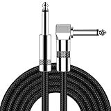
- [Low Noise High Fidelity] New bee guitar cord with 22AWG oxygen-free-copper center conductors provides enhanced signal transfer, the PVC insulation material and the high-density stranded copper double shield provide noise rejection for quiet operation
- [Ideal for Choice] New bee 1/4 straight and right angle metal connectors, ensures a secure connection in any instrument, pedal, or amp jack. L shape great fro on stage guitar stands
- [Wide Compatible] Suitable for mixer, power amplifier, microphone, effector, decoder, equalizer, electoronic organ, electric guitar, electric bass and other electronic equipments. Widely used in the installation of smart home, karaoke speaker, professional stage audio, etc
- [Easy Disassemble] Making incidental repairs quick and easy! Very nice, flexible cable
- [Dont Hesite to Order] 24 hours customer services and professional technology team are standing by
Doping both n-type and p-type devices
Complementary logic needs reliable n- and p-channel transistors. The 300 mm demonstration paired MoS2 nFETs with WS2 or WSe2 pFETs, but a research demonstration is not yet a mature, high-volume doping flow. Stable, spatially uniform doping that survives subsequent processing remains difficult.
Do these 3 things before closing this tab:
1Fix the driver behind crashes, sound loss and screen glitches2Clear out junk files and repair common Windows errors3Scan for outdated or missing drivers - takes under a minuteDielectric interfaces and traps
A gate dielectric must control the channel without introducing excessive charge traps. The National Science Review perspective reports that dielectric interface trap density in 2D devices can still exceed that of the Si–SiO2 interface by about two orders of magnitude. Traps can shift threshold voltage, increase hysteresis, reduce mobility and create reliability failures, particularly when the device is repeatedly switched.
Transfer, contamination and thermal budget
Many 2D films are grown or processed under conditions that do not fit directly into an established CMOS sequence. Moving a fragile film onto a production wafer can create wrinkles, residue, tears or contamination. A viable flow must also accommodate patterning, vias, deposition, atomic-layer processing, polishing, passivation and encapsulation while staying inside the thermal and contamination budgets of the surrounding circuitry.
Metrology, inspection and reliability
NIST describes the lab-to-fab transition as early and says there is no one-size-fits-all metrology solution. Fabs need measurements for thickness, composition, crystal structure, electrical behavior and mechanical integrity, linked to defect maps and final circuit performance. They also need wafer-level statistics, accelerated lifetime tests and agreed pass/fail criteria. Without those tools, a reported yield from one experiment cannot be compared directly with a production line’s yield metric.
Circuit density and design infrastructure
A transistor is only one element in a chip. Designers need compact models that capture variation, design rules for 2D-specific contacts and spacing, standard-cell libraries, interconnect schemes and process-design kits. The gap in demonstrated system scale is large: a National Science Review perspective cites a 1-bit MoS2 microprocessor containing 115 transistors in 0.6 mm2, whereas state-of-the-art CMOS CPUs contain more than 10 billion transistors in roughly 100 mm2. That comparison is not a like-for-like benchmark, but it shows how far circuit integration must advance.
Rank #4

- Digital Family Calendar: BSIMB digital calendar wall touch screen puts an end to your chaotic life. Designed for busy families, the digital calendar keeps you organised and in step with your family. Assign different colours and tasks to each family member to make family scheduling easier and more intuitive.
- Easy Setup and Auto-Sync: Plug in, connect to WLAN and auto-syn your electric calendar in minutes. Digital wall calendar compatible with Google calendar, iCloud calendar, Outlook calendar, Cozi calendar and Yahoo calendar. Add events directly on the device or through the ecalendar app. Electronic calendar stays current whether you're at work or traveling—no manual updates needed.
- All-In-One Home Assistant: Smart calendar builds habits and encourage independence with personalised chores. Display daily meal plan to reduce the daily ‘What's for dinner?’ stress. To-do lists keep track of everything you want. Turning chores into valuable achievements with stars and rewards, making life easier and more enjoyable.
- Manage Anytime Anywhere: BSIMB electronic calendar for family stay connected with the powerful ecalendar app. Access and manage your digital wall calendar anytime, anywhere with free features like stars & rewards, photo screensaver, chore charts, meals plans, to-do lists etc. Electronic planner paid features like Magic Import tailor advanced tools for users with special needs.
- Stay in Touch with Loved Ones: Share photos or videos from your phone to electronic wall calendar with app, instantly update your life moment, and keep in touch with your family, especially those who are far away; you can also surprise your smart calendar digital wall by sending him a wish card; it's also great for keeping tech-illiterate elders in touch with the youngsters.
Can MoS2 replace silicon?
MoS2 is better viewed as a possible complement to silicon than as an imminent replacement. Silicon has a mature supply chain, decades of reliability data, established design automation, enormous installed capacity and highly optimized interconnects. Replacing it would require 2D technology to match not only transistor characteristics but also complete manufacturing ecosystems.
The strongest case for MoS2 is where its atomic thickness solves a problem that bulk silicon cannot solve efficiently: electrostatic control at extremely small dimensions, low-temperature integration on a finished wafer, or vertical placement above existing circuitry. In those roles, a smaller number of 2D transistors could provide a system-level advantage even if they do not displace silicon logic everywhere.
Are 2D semiconductors better than silicon at a “2 nm” node?
“2 nm” is a process-generation label, not a promise that every transistor dimension is 2 nm. Comparing a 2D transistor with a silicon transistor solely by that label is misleading. The relevant comparison includes contacted poly pitch, gate length, contact resistance, drive current, leakage, variability, interconnect delay, thermal behavior and manufacturing yield.
The 300 mm demonstration used channel lengths as small as 28 nm and a 50 nm contacted poly pitch; those are concrete dimensions, but they do not constitute a commercial 2 nm product. Likewise, a high laboratory mobility does not guarantee higher chip performance when contacts, dielectric traps, wiring and variability are included. 2D channels may become advantageous at future scaled or vertically integrated nodes, but current evidence does not show that they are broadly better than silicon in production.
Quick wins for a faster PC:
Clear out junk files and repair common Windows errorsFree Scan →Fix the driver behind crashes, sound loss and screen glitchesFind Drivers →Where commercial adoption is most plausible first
Early products are more likely to use 2D transistors in targeted roles than in general-purpose CPUs. The most plausible areas are:
- Low-power electronics: IRDS roadmaps summarized by NIST place the clearest high-volume insertion case in low-power applications.
- Back-end-of-line and wafer-backside devices: atomically thin channels can potentially be added above or behind silicon circuitry at temperatures compatible with completed wafers.
- Heterogeneous 3D integration: a 2D layer could provide logic, sensing or control directly over another semiconductor tier, shortening connections.
- Sensors and specialized interfaces: the exposed or easily functionalized surface of a 2D material can be useful where detecting a chemical, optical or biological signal matters more than maximum digital density.
- Ultra-scaled research logic: applications that tolerate a new process and value very small footprints may adopt the technology before mainstream processor makers do.
These niches still require qualification, packaging and supply-chain work. “First use” should therefore be understood as a likely insertion point, not a guaranteed product schedule.
When might 2D-material chips become available?
There is no defensible single launch date. Industrial research and pilot-line demonstrations are active in 2026. NIST summarizes an IRDS expectation that 2D materials could enter high-volume manufacturing mainly for low-power applications within the next ten years. A National Science Review perspective cites an IRDS projection for 2D channels at 0.7 nm nodes in 2034.
Both statements are roadmap targets, not commitments. A realistic sequence is: process demonstrations and metrology development first; specialized pilot products next; broader volume insertion only after reliability, design enablement, cost and supply-chain evidence are established. Delays in any one of those areas can move the schedule by years.
How to judge the next commercial-readiness claim
When a company or research consortium announces a new result, look for the following details rather than a headline mobility number:
- Wafer diameter, number of wafers and whether the process used commercial production equipment.
- How yield is defined, including the electrical pass criterion and the fraction of devices tested.
- Thickness, composition and defect uniformity across the wafer.
- Contact resistance and current density at the stated contacted pitch and channel length.
- Separate results for nFETs and pFETs, plus evidence that complementary circuits operate together.
- Dielectric trap density, hysteresis, bias-temperature stress and lifetime data.
- Thermal budget, transfer steps, contamination controls and compatibility with existing CMOS layers.
- Demonstrated circuit size, defect tolerance, interconnect performance and availability of design models.
- Cost, throughput and a credible source of production-grade materials and equipment.
A result that supplies those numbers is more informative than one that reports only the best transistor in a small test array.
Bottom line
2D-material transistors are promising and increasingly fab-compatible, but they are not yet a mainstream commercial replacement for silicon. The 200 mm and 300 mm demonstrations show that wafer-scale processing, complementary device integration and aggressive dimensions are achievable. The remaining work is broader: uniform materials, low-resistance contacts, stable doping, low-trap dielectrics, contamination-safe integration, metrology, reliability, dense circuits and a complete design ecosystem must all mature together before high-volume products become routine.
Quick Recap
Product prices and availability are accurate as of the date/time indicated and are subject to change. Any price and availability information displayed on Amazon at the time of purchase will apply.
Free tools Windows power users keep installed
One-click scans. No signup required.

