Quick wins for a faster PC:
Scan for outdated or missing drivers - takes under a minuteDriver Scan →Repair Windows errors before they cause bigger problemsFix Now →AI can help with discrete parts of printed circuit board (PCB) design, including interpreting schematics, exploring component placement, and coordinating analysis tools. It does not, by itself, establish that a board is electrically sound, manufacturable, or ready to build. Current examples range from vendor-described software features to preprint experiments on narrow tasks; they do not establish a generally applicable time saving for designing and prototyping a complete PCB.
Which parts of PCB design can AI accelerate?
A PCB workflow runs from circuit definition through layout, verification, testing, and assembly. AI tools target selected steps in that chain. Their usefulness depends on the task, how well they connect to existing EDA software, and whether their output can be checked with established engineering tools.
As an Amazon Associate I earn from qualifying purchases.
Turning schematic images into circuit data
A schematic-to-netlist system can interpret an image, identify components and their labels, infer connections, and produce a netlist: a machine-readable description of which pins belong to which electrical nets. That can help convert existing drawings into data that downstream design tools can use.
The Tool Desk
Outbyte Driver Updater FREEScan for outdated or missing drivers - takes under a minuteDriver Scan →Outbyte PC Repair FREEClear out junk files and repair common Windows errorsFree Scan →The authors of the 2026 SINA preprint report 96.67% overall netlist-generation accuracy in their experiments and say their result was 2.72 times higher than the state-of-the-art approaches they compared against. Both figures apply to the authors’ netlist-generation task and experimental setup. They are not measures of complete-board accuracy, prototype success, or time saved across an engineering project.
#1 Best Overall
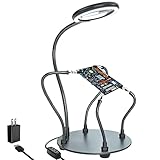
- Helping hands soldering station with magnifying Lamp: soldering kit, very suitable for welding, assembly, maintenance, modeling, hobbies, jewelry, and crafts. With a sturdy and flexible metal hose arm and a dimmable magnifying glass, the circuit board can be fixed to the best position you want.
- Illuminate and magnify your field of vision: The 3X dimmable magnifying lamp has 28 lamp beads with 500 lumens illuminance, which can be switched between 6 brightness levels at will. It can help you to illuminate and magnify the tiny details while you are working, so as to ensure the accuracy and accuracy of the work as much as possible
- Sturdy gooseneck and insulated alligator clips: 2 adjustable 7.5-inch and 2 adjustable 5-inch metal gooseneck arms(soldering hands), which are tightly locked on the base by screws. The alligator clips can be rotated 360 degrees, and then positioned and locked in place. The clip is equipped with a rubber sleeve, so you can avoid scratching the polished surface of the jewelry or avoid short circuits.
- Heavy-duty base: A round powder-coated steel base with a diameter of 7 inches ensures that your solder stand will not tip over. There are 4 non-slip rubber pads on the bottom to prevent the welding assistant from sliding on the workbench.
- The package includes: 1 x solid metal base, 1 x LED magnifying glass, 4 x flexible arm with alligator clip, 4 x rubber cover, 4 x Phillips screws, 1 x US plug, 1 x mini wrench, 1 x mini Phillips screwdriver, 1x cleaning cloth, 1x user manual.
Exploring placement and layout
Component placement affects the geometry and quality of a board, so it is a natural target for optimization. NVIDIA’s EDA research page identifies Bayesian optimization, reinforcement learning, and generative AI among its explored methods. It also notes that Cypress, a GPU-accelerated PCB placement paper, received the Best Paper Award at ISPD’25 in March 2025. That is evidence of active work on placement—not proof that an AI placement method is best for every board or production workflow.
Siemens says its Fuse EDA AI Agent can assist PCB layout through its Xpedition and HyperLynx tools. That is a vendor description of product capability, rather than an independently measured comparison of design time or board quality.
Routing traces and optimizing a board
Routing connects electrical nets with copper traces while respecting board constraints. AI methods can help search for or optimize candidate solutions, but a plausible-looking route is not necessarily a valid one. Trace geometry and connectivity must satisfy the relevant design rules and the project’s electrical requirements.
The 2026 PCBWorld preprint describes a benchmark environment that uses KiCad engine operations and native design-rule-check feedback. Its abstract says learning-based routing methods still lag rule-based routers in the setting it examines. That finding cautions against assuming that AI routing is universally faster or better; it does not establish a result for every router, board type, or design constraint.
Rank #2

- 【2-IN-1 SOLDERING STATION & HOT AIR REWORK STATION】 Combine two essential electronics repair tools in one compact workstation. This 2-in-1 soldering station features a precision soldering iron and hot air rework gun for SMD soldering, PCB repair, IC rework, desoldering, component removal and electronics DIY projects. The space-saving design is ideal for circuit board repair, electronic repair, mobile phone repair, motherboard repair and general soldering work, giving hobbyists and technicians one versatile solution for everyday rework tasks.
- 【DUAL LCD DISPLAY & INDEPENDENT TEMPERATURE CONTROL】 Monitor the soldering iron and hot air rework gun with clear dual digital LCD displays and adjust each function independently. The PID temperature control system helps maintain stable and consistent heat during delicate soldering and rework operations. Whether performing SMD component soldering, PCB board repair, IC replacement, desoldering or precision electronics repair, independent temperature adjustment gives you better control for different components and applications.
- 【FAST HEATING & PRECISE SMD REWORK】 Designed for efficient electronics repair with rapid heating and controlled heat output. The hot air rework function is suitable for SMD component removal, IC desoldering, circuit board repair, chip rework and electronic component replacement, while the soldering iron handles precision solder joints and through-hole or PCB soldering tasks. A practical choice for SMD rework stations, PCB repair stations, electronics workbenches and DIY soldering projects.
- 【AUTO SLEEP, AUTO COOLING & ESD SAFE DESIGN】 Built with convenient features for safer and more efficient daily use. The auto sleep function helps reduce unnecessary heating during idle periods, while the auto cooling function helps cool the system after operation. ESD anti-static protection is designed for work involving sensitive electronic components. Ideal as an ESD safe soldering station, electronics repair station, SMD rework station and PCB soldering station for makers, technicians and electronics enthusiasts.
- 【VERSATILE ELECTRONICS REPAIR TOOL FOR DIY & PROFESSIONAL USE】 A versatile digital soldering and hot air rework station for a wide range of applications, including PCB repair, SMD soldering, IC rework, circuit board repair, electronic component removal, mobile phone repair, computer repair, motherboard repair and DIY electronics projects. The compact 2-in-1 design saves valuable workbench space while providing both soldering and hot air rework capabilities for hobbyists, makers, repair technicians and electronics professionals.
Coordinating analysis and design tools
Complex EDA work can involve multiple tools and repeated handoffs between design, verification, and manufacturing sign-off. Siemens announced Fuse EDA AI Agent on March 16, 2026, describing it as a way to orchestrate workflows across those activities. For PCB systems, Siemens says the agent can assist with layout, signal integrity, and other analyses through Xpedition and HyperLynx.
Workflow orchestration may reduce repetitive tool coordination, but the announcement does not provide an independently audited PCB-project speedup. Siemens’ June 23, 2025 announcement also described generative and agentic AI features, customizable workflows, access controls, and cloud or on-premises deployment. For teams handling proprietary board data, deployment location and access controls are practical evaluation criteria—not evidence of a particular productivity gain.
Does AI make PCB prototyping faster?
It may shorten parts of the design-iteration process if it helps an engineer create or revise candidate design data, explore alternatives, or coordinate analyses. But “prototyping” can mean different things: preparing a board design for fabrication, producing a physical board, assembling it, or testing the completed circuit. The cited examples focus on design tasks and workflow automation; they do not establish an end-to-end reduction in the time or cost of fabricating and validating physical prototypes.
Windows Errors? Fix Them Before They Spread
Repair common Windows errors and clear accumulated junk for a smoother, more stable PC - no reinstall needed.Free scan · no reinstallCrashes, No Sound, or Screen Glitches?
Random freezes, missing sound and display glitches usually trace back to one bad driver. Find and replace yours safely.Free scan · under a minuteThe 2025 preprint survey, Surveying GenAI-based Automation in Printed Circuit Board Design and Test, covers AI work across system specification, circuit design, layout, optimization, validation, testing, assembly, and distribution. It also identifies domain-specific data scarcity and limited integration with existing PCB tools as challenges. Those limits matter in practice: an assistant that cannot reliably use a team’s design files, constraints, and verification flow may create more review work than it removes.
Rank #3

- ESD Safety Anti-Static Mat:This is high-quality ESD repair mat. The resistivity of the esd mat is 10⁶ Ω, which can effectively prevent the generation and accumulation of static electricity, control the generation of static electricity, and quickly lead the generated static electricity into the ground wire, reducing the risk of electrostatic breakdown of electronic products and providing a safer and better working environment for the assembly, repair or soldering of sensitive electronic products
- Increase working Size and Multi-Function:The 21.6 x 16.9 Inch silicone soldering mat large has the size of the largest repair area at present,solder mat has 48 built-in screw&parts storage positions,which can keep the removed small parts in good classification and easier to obtain.You don’t have to worry about losing small screws or precision parts repair tools during the repair process, thereby improving work efficiency and keeping the repair platform tidy
- ESD Accessories for Grounding:Kaisi antistatic mat for electronics contains a set of ESD accessories.it includes grounding plug, grounding wire and ESD wrist strap. These ESD accessories are very convenient for you to connect the antistatic mat to the ground. When static electricity is generated, ESD repair mat can quickly introduce static charge into the ground, providing a stable and reliable maintenance platform for maintenance personnel, ensuring the integrity of electronic equipment
- Heat Resistant 932℉ Soldering Mat:Large soldering mat heat resistant can withstand high temperatures up to 932°F (500°C),are corrosion-resistant,and have a soft texture to protect your workbench from burning and damage.Soldering irons and hot air workstations can directly contact the silicone work pad, which can directly support high-temperature soldering work
- Big Size Design More Widely Used:This lager anti static mat is carefully designed to increase the area of the work area.You no longer have to worry about the mat is too small to complete work. antistatic mats can provide more space to meet the repair needs of lager electronic devices and soldering projects, such as pc building, repair computer, laptop, MacBook,iPad,iphone,drone,PCB,raspberry PI and diy
What AI output does—and does not—prove
AI-generated or AI-assisted design work should be treated as a candidate for engineering review. A netlist, placement, route, or analysis result does not by itself prove that a board is correct or ready to manufacture.
- Connectivity: confirm that the netlist and schematic express the intended circuit.
- Design rules: run the EDA tool’s checks against the actual board constraints and resolve violations rather than relying on a generated suggestion alone.
- Electrical behavior: review relevant signal-integrity and other analyses for the design’s operating requirements.
- Manufacturability and function: assess fabrication and assembly requirements, then test the physical board as appropriate.
The PCBWorld preprint’s use of native design-rule-check feedback illustrates how an automation environment can be grounded in an EDA engine. A passing check is still only one part of validation; it is not a substitute for reviewing the requirements and behavior that the checks do not cover.
How to evaluate an AI feature in your own workflow
Judge a feature on a bounded task before trusting it with a full project. A practical evaluation can separate time saved from work shifted into checking and repair.
What’s actually slowing this PC down?
Pick the symptom - the matching free tool is one click away.
- Choose one task. For example, test schematic-image conversion, placement suggestions, routing, or workflow coordination rather than treating “PCB design” as a single capability.
- Set a baseline. Record how the team handles that task today, including review and correction time. Use the same design inputs and constraints when comparing an assisted workflow.
- Check integration. Confirm that the feature works with the team’s EDA tools, design data, constraints, and handoffs. The 2025 survey identifies limited integration with existing PCB tools as a field-wide challenge.
- Validate the output. Use the appropriate EDA checks and engineering review. Track defects, corrections, and any work the AI feature creates as well as the time it appears to save.
- Review data handling. For proprietary designs, establish where data is processed, who can access it, and what deployment options and controls apply. Product-specific arrangements should be checked with the vendor.
When weighing evidence, keep task-level experiments separate from product descriptions. SINA’s reported accuracy concerns netlist generation in its experiments; NVIDIA’s page describes EDA research activity; and Siemens’ announcements describe its own product capabilities. None supplies a generally applicable, independently verified figure for how much faster a complete PCB design-and-prototype cycle will be.
Quick Recap
Product prices and availability are accurate as of the date/time indicated and are subject to change. Any price and availability information displayed on Amazon at the time of purchase will apply.




