The Tool Desk
Outbyte PC Repair FREEClear out junk files and repair common Windows errorsFree Scan →Outbyte Driver Updater FREEScan for outdated or missing drivers - takes under a minuteDriver Scan →Tape automated bonding (TAB) connects a semiconductor die to patterned metal leads on a flexible polymer tape. The tape’s inner leads bond to the die; its outer leads connect onward to a package, substrate, or circuit. This arrangement can support fine-pitch connections and temporary electrical testing during assembly.
What tape automated bonding means
TAB is a semiconductor die-interconnection and assembly process. A flexible tape carrier holds patterned conductors, commonly copper on a polymer such as polyimide. The die is aligned and bonded to the conductors, which carry its electrical connections to the next part of the assembly.

As an Amazon Associate I earn from qualifying purchases.
IEC 60191-5:1997 describes TAB as an assembly process for integrated circuits used without conventional packages, with the silicon chip exposed. That wording comes from the standard description reproduced in a standards catalog; it captures one application, while TAB’s broader role is to connect a die through tape-carried leads.
How the process works
The exact sequence depends on the design and manufacturing process. A typical flow includes these stages:
#1 Best Overall

- We are providing high quality research grade Indium metal foil. Purity >=99.995%; Thickness: 0.3mm Width: 50mm (Approx. 1.968 inch) Length: 50mm (Approx 1.968 inch)
- This item is vacuum packed. Maintained original appearance of Indium metal and avoided oxidation. Color of this Indium foil is shiny silvery white;
- We can do customized size of this material. If you have different needs please send us a message and we will help you complete the transaction;
- It's great for CPU heat sink, bonding, laboratory science experiments, research and semiconductor technology production purpose using. It also can be a great gift for element specimen collectors;
- It's mainly used for low-temperature vacuum sealing, cooling of high-end equipment and fuel cells. clean and non-oxidized indium foil surface be required;
- Prepare the die: A wafer is separated into individual dies.
- Index the tape: A flexible carrier with patterned conductors is positioned at the bonding station. Alignment holes can help register the tape.
- Align the inner leads: The die’s pads or bumps are aligned with the tape conductors. The die-to-tape connections are called inner-lead bonds (ILB).
- Make the bond: The bonding method depends on the process. In thermocompression gang bonding, a thermode applies heat and pressure to join multiple aligned leads in one operation.
- Test when applicable: Temporary test pads can provide electrical access to the die and tape assembly during production.
- Connect the outer leads: The tape leads are joined to a lead frame, package, substrate, or external circuit. These are outer-lead bonds (OLB).
What the tape and connections are made of
TAB tape commonly combines a flexible polymer carrier, such as polyimide, with patterned copper conductors. A cited industry overview also describes single-sided tape and constructions with two metal layers. At the die connection, bumps or balls may be used; gold and solder are examples in the cited overview, not a universal materials specification.
The conductor pattern defines where electrical connections run. Alignment features support registration, while temporary test pads can provide test access before the outer leads are connected to the next assembly level.
Rank #2
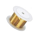
- Product Name: high purity gold wire
- Purity: Au ≥ 99.99%
- Gold thread material: Au 99.99% gold content, microelement 0.01%. It can be used in electrode experiment, scientific research, machinery, aerospace, electronics and other industries
- Function of gold wire: gold wire is a kind of internal lead material with excellent electrical, thermal conductivity, mechanical properties and chemical stability. It is mainly used as the key packaging material of semiconductor. It plays the role of wire connection in LED packaging, connecting the chip surface electrode and bracket. When conducting current, the current enters the chip through the gold wire to make the chip glow;
- Advantages of gold wire: it has large conductivity, corrosion resistance, good toughness, and is widely used in integrated circuits. Compared with other materials, the biggest advantage is oxidation resistance.
Why use TAB, and what are its trade-offs?
Industry descriptions identify several potential advantages: fine-pitch bonding and smaller pads, the option to place bond pads across more of the die rather than only around its edge, a higher possible I/O count for a given die size, reduced gold use, and less variation in bonding geometry. These are process capabilities, not guarantees for every TAB design.
Free tools Windows power users keep installed
One-click scans. No signup required.
TAB is one choice among die-interconnection methods, including wire bonding and flip-chip bonding. There is no universal winner: the appropriate process depends on the package and manufacturing requirements.
| Decision factor | What to assess |
|---|---|
| Pitch and connection geometry | Whether the design needs fine-pitch connections, small pads, or connections distributed across the die. |
| I/O density | How many connections the die needs relative to its size and layout. |
| Assembly throughput and sequence | Whether the production flow benefits from bonding multiple leads together and how the steps fit the line. |
| Test access | Whether temporary tape test pads are useful before final connection to the package or substrate. |
| Package and substrate requirements | How the tape’s outer leads connect to the rest of the assembly. |
| Materials, tooling, and rework | Whether the required tape, bonding equipment, manufacturing infrastructure, and rework approach suit the application. |
A historical account says TAB use peaked from the 1980s to the early 1990s, when fine-pitch gold thermosonic wire bonding capability and wire-bonding throughput were more limited. This is historical context, not current adoption or market-share data.
Independent reader supportYour contribution helps us test, update, and keep practical guides available for everyone.How TAB differs from wire bonding
The main distinction is the form of the die connection. TAB bonds the die to patterned leads carried on flexible tape; wire bonding connects die pads to other conductors using individual wires. TAB’s tape pattern can support fine-pitch connections and gang bonding, while wire bonding uses wire-by-wire interconnections. Which approach fits better depends on pitch, I/O density, package design, test access, production flow, equipment, materials, and rework needs; the available evidence does not establish a universal performance ranking.
Quick Recap
Rank #4

- KW-4B type coating machine is suitable for semiconductor wafers, slides, wafer, substrate, LED, photovoltaic industry, ITO conductive glass plate surface coating process.
- The product has the advantages of stable speed and rapid start-up, and can ensure the consistency of coating thickness and uniformity of semiconductor materials.
- Normally used with vacuum pumps. Small size can be placed in the glove box.
Product prices and availability are accurate as of the date/time indicated and are subject to change. Any price and availability information displayed on Amazon at the time of purchase will apply.




