What’s actually slowing this PC down?
Pick the symptom - the matching free tool is one click away.
AI chips are advancing through more than smaller transistors. Designers are combining new transistor structures with chiplets, high-bandwidth memory, advanced packaging and, in research, optical interconnects. The aim is to move data efficiently between compute and memory while controlling power, heat, yield and cost. This is what “beyond Moore’s Law” means: adding routes to progress, not declaring transistor scaling over.
Why AI computing needs more than smaller transistors
AI workloads put pressure on the whole system. Processing speed matters, but so do the energy required to move data, the amount of memory near a processor, and the heat a package can dissipate. The U.S. Department of Energy identifies miniaturization, processing speed, power consumption, thermal management and operating environment as interconnected microelectronics challenges.



As an Amazon Associate I earn from qualifying purchases.
The Semiconductor Industry Association’s 2025 overview likewise describes progress across software, materials, design, architectures and packaging, alongside continued scaling. Its application goals include low power, high bandwidth, lower latency, thermal stability and higher-voltage operation. These are directions for innovation, not guaranteed outcomes for every chip or workload.
Quick wins for a faster PC:
Repair Windows errors before they cause bigger problemsFix Now →Scan for outdated or missing drivers - takes under a minuteDriver Scan →Clear out junk files and repair common Windows errorsFree Scan →What “beyond Moore’s Law” means
Moore’s Law is commonly used as shorthand for the long-running trend of increasing transistor counts on integrated circuits. It is not a promise that every new chip will be faster, cheaper or more efficient by a fixed amount. Nor does “beyond Moore’s Law” mean that transistor scaling has stopped. It describes the broader set of ways engineers can improve a computing system when transistor scaling alone does not address its bottlenecks.
#1 Best Overall
That broader approach can involve changing the transistor, separating power delivery from signal routing, assembling multiple dies in one package, bringing memory closer to compute, or exploring optical links. A process-node name is a manufacturing-generation label; it should not be read as a literal measurement of every transistor feature.
How transistor and power-delivery designs are changing
Gate-all-around and nanosheet transistors
In a gate-all-around design, the gate surrounds the transistor’s channel, providing a different way to control it than earlier structures. Nanosheet implementations use stacked, sheet-like channels. Intel describes its RibbonFET approach as a gate-all-around transistor, while TSMC describes its own transistor and process roadmap separately. Any performance or power improvements attributed to these approaches are vendor claims, not a neutral head-to-head benchmark in the available evidence.
Backside power delivery
Conventional layouts route power and signals through the front side of the silicon. Backside power delivery moves power connections to the rear, aiming to separate power routing from signal routing and free space on the front side. Intel describes its PowerVia technology in these terms. TSMC’s April 24, 2024 announcement included a backside power rail in its A16 plan. That announcement records a historical plan; it does not by itself establish the technology’s present production status.
Do these 3 things before closing this tab:
1Repair Windows errors before they cause bigger problems2Scan for outdated or missing drivers - takes under a minute3Clear out junk files and repair common Windows errorsRank #2

- FAST RUNS IN THE FAMILY — The 14-inch MacBook Pro with the M5 Pro or M5 Max chip brings next-generation speed and powerful on-device AI to personal, professional, and creative tasks. With all-day battery life, double the starting storage,* and a breathtaking Liquid Retina XDR display, it’s pro in every way.*
- BUCKLE UP — Along with a next-generation CPU, faster unified memory, and up to 2x faster SSD storage,* M5 Pro and M5 Max feature a more powerful GPU with a Neural Accelerator built into each core, delivering faster AI performance and on-device training capabilities. So you can blaze through demanding workloads at mind-bending speeds.
- BUILT FOR AI — Apple silicon, and every major component that powers it, is designed to run demanding on-device AI workloads like LLM inference and training. And Apple Intelligence helps you write, express yourself, and get things done effortlessly with groundbreaking privacy protections at every step.*
- ALL-DAY BATTERY LIFE — MacBook Pro delivers the same exceptional performance whether it’s running on battery or plugged in.*
- MACOS RUNS APPS FAST — All your go-to apps run lightning fast in macOS, including built-in apps like FaceTime and Messages. Plus, built-in virus protection and free software updates help keep your Mac running smoothly and securely.
How chiplets and packaging build a larger system
Chiplets split a design into connected dies
A chiplet system combines multiple smaller dies within one package rather than putting every function on one large die. The dies may use different process generations or come from different sources, depending on the design. This modular approach can help assemble a larger system from specialized components, but it adds design and integration decisions: the dies must communicate through package-level connections, and the package must manage their power and heat.
Intel says smaller chiplets can be easier to yield than very large dies approaching reticle size. That is Intel’s description of its approach, not a universal yield result: manufacturing outcomes depend on the design, process and packaging choices.
2.5D, 3D and bridge-based integration are distinct approaches
“Advanced packaging” covers several ways of connecting dies; it does not name one specific construction. In a 2.5D arrangement, dies sit side by side and connect through an interposer or another dense package-level structure. In 3D integration, dies are stacked vertically. Bridge-based designs connect nearby dies with a local bridge rather than treating the entire package as one interposer surface.
Rank #3
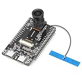
- 【Main Functions】BW21-CBV-Kit is a local AI vision recognition development board capable of independently running object recognition models
- 【Camera Specifications】Equipped with a 1920 x 1080 resolution, 2MP, 30fps wide-angle camera, a condenser microphone, and support for 2TB memory card storage
- 【Strong Communication Capabilities】Based on the RTL8735B chip, it supports dual-band 2.4GHz/5GHz WiFi and Bluetooth 5.1, providing high-performance wireless transmission capabilities for smoother image transmission
- 【Development Method】Utilizes the Arduino development approach, allowing you to easily implement your ideas, such as face recognition, gesture recognition, object recognition, component defect detection, people counting, pet recognition, etc
- 【Rich Interfaces】Two sets of 18-pin headers provide 30 programmable I/Os, facilitating project expansion. Combined with AI recognition, it unlocks limitless possibilities
Intel describes EMIB as a 3.5D packaging approach and Foveros Direct as a 3D stacking technology. TSMC describes CoWoS as placing processor chips and high-bandwidth memory stacks on an interposer, and SoIC as a 3D stacking solution. These are vendor descriptions of different integration methods, not results from a neutral comparison.
Why hybrid bonding matters
Hybrid bonding is a way to connect stacked components at very fine pitch. IBM Research describes work on hybrid bonding alongside packaging that brings multiple technologies together for AI and logic. IBM also reports that its Bromont facility manufactures 100,000 advanced flip-chip modules each week. That figure is IBM’s stated output for that facility, not an industry-wide production statistic.
Why high-bandwidth memory is part of the package story
AI processors need to exchange large amounts of data with memory. High-bandwidth memory, or HBM, uses stacked memory dies and is commonly integrated close to compute in advanced packages. TSMC’s description of CoWoS places processor chips and HBM stacks on an interposer, illustrating how packaging can provide dense connections between them.
Bringing memory close to the processor addresses the connection between compute and memory; it does not make every workload faster automatically. Capacity, bandwidth, power, package complexity and supply availability all matter. The evidence available here does not establish a neutral comparison of HBM implementations or their costs.
Independent reader supportYour contribution helps us test, update, and keep practical guides available for everyone.Photonics and other research-frontier directions
Silicon photonics and co-packaged optics
Silicon photonics and co-packaged optics aim to move data optically closer to computing components, rather than relying only on electrical connections. Potential evaluation questions include link bandwidth, energy per transfer, reach, packaging complexity and manufacturing maturity. TSMC and IBM identify optical integration as a development or research direction. TSMC’s April 2024 announcement included target dates for silicon photonics and co-packaged optics; those historical targets should not be treated as confirmation of availability in 2026.
New materials and quantum-related microelectronics
Materials research can broaden the options for building or operating microelectronics. The Department of Energy identifies advanced materials, nanofabrication and quantum-related capabilities such as cryogenics among its research areas. These are research capabilities and goals, not evidence that such technologies are widely deployed as drop-in replacements for commercial AI processors.
Best Value
The Department of Energy also proposes an AI-driven, full-stack co-design ecosystem to accelerate materials and manufacturing research and development. This is a research direction that connects design choices to materials and manufacturing; it is not a claim that AI has removed the physical or economic constraints on chip production.
How to assess an AI-era semiconductor approach
There is no universally best architecture in the cited material. A useful comparison starts with the workload and asks where its actual bottleneck lies, then evaluates the system rather than a single component.
- Workload fit: Identify whether the limiting factor is computation, memory capacity, data bandwidth, latency or a mix of them.
- Power and heat: Consider energy use under the intended operating conditions and whether the chip and package can dissipate the resulting heat.
- Memory and interconnect: Check whether memory bandwidth, capacity and connections between dies match the workload’s needs.
- Manufacturing readiness: Distinguish technologies described as shipping or established from vendor roadmaps and research-stage proposals. A dated announcement is not current availability evidence.
- Yield and design complexity: Ask how multiple dies are tested and integrated, and how package complexity affects manufacturing risk.
- Cost: Include the package and system, not just the compute die. The sources do not provide comparable cross-vendor costs, yields or performance-per-watt benchmarks.
Vendor statements can explain how a company says its technology is designed to work, while association and government materials describe broader priorities and research goals. None of the cited sources supplies a current, neutral cross-vendor benchmark that settles performance, efficiency, cost or deployment maturity across these approaches. A sound decision therefore depends on workload-specific evidence, not on a technology label alone.
The Tool Desk
Outbyte Driver Updater FREEFix the driver behind crashes, sound loss and screen glitchesFind Drivers →Outbyte PC Repair FREEClear out junk files and repair common Windows errorsFree Scan →Quick Recap
Product prices and availability are accurate as of the date/time indicated and are subject to change. Any price and availability information displayed on Amazon at the time of purchase will apply.




