3D chip stacking places dies or wafers above one another and connects them vertically, bringing selected chip functions closer together. It can increase functional density and shorten data paths, helping chip designers pursue bandwidth, performance, power, and footprint goals. It does not make transistors smaller, and it is not a universal replacement for transistor scaling.
What 3D chip stacking means
A conventional chip lays its circuits across a mostly flat silicon surface. In 3D integration, designers place some components above others and link them with vertical electrical connections. The result can put compute, memory, I/O, or other functions closer together than a design spread across a single plane.
As an Amazon Associate I earn from qualifying purchases.
Think of a building with several floors connected by short lifts instead of one building with every room spread over a huge footprint. That illustrates the geometry, not the manufacturing challenge: a real stack must account for heat, power delivery, alignment, interconnects, and production yield.
Quick wins for a faster PC:
Scan for outdated or missing drivers - takes under a minuteDriver Scan →Clear out junk files and repair common Windows errorsFree Scan →The term “3D stacking” can refer to different levels of integration. These approaches are related, but they are not interchangeable:
#1 Best Overall

- Up to 16 Colors: Bring your designs to life with vibrant multi-color/multi-material printing capabilities, perfect for showcasing your creativity. Note: Connecting Bambu Lab AMS is required.
- 500mm/s and 20000 mm/s² Acceleration True High Speed: Don't wait around for your masterpieces. Lightning-fast printing speed lets you focus on creating, not waiting.
- Enclosed Design: Fully enclosed body improves print performance for advanced filaments. Automatic Bed Leveling: Say hello to high-quality, successful prints. Auto bed leveling makes 3D printing such an easy thing.
- Set Up in 15 Minutes: Spend more time printing and less time setting up. User-friendly design ensures a hassle-free assembly experience for all skill levels.
- Supported Filament: Ideal: PLA, PETG, TPU, PVA, PET ABS, ASA; Capable : PA, PC; Not Recommended: Carbon/Glass Fiber Reinforced Polymer.
- Die or chiplet stacking: separate dies are assembled above one another in a package.
- Wafer-level 3D integration: integration takes place at the wafer level, as in TSMC’s [SoIC overview].
- Transistor-level stacking: transistor device layers are built above one another. This is a distinct device-architecture approach, not simply another name for stacking packaged chiplets.
Why stack chips when planar scaling gets harder?
As computing systems grow, moving data between compute and memory can consume time, energy, and physical area. Bringing selected functions closer and connecting them with dense vertical links gives architects another way to improve a system, alongside improving the transistors in each layer.
Intel describes Foveros as a way to place high-performance logic chiplets above a base die that can contain I/O, SRAM, and power-delivery circuits. In Intel’s 2018 announcement introducing Foveros, the company said: “It will allow products to be broken up into smaller ‘chiplets,’ where I/O, SRAM and power delivery circuits can be fabricated in a base die and high-performance logic chiplets are stacked on top.” This is Intel’s description of its architecture and intended flexibility.
Shorter connections and denser integration can support higher bandwidth or lower communication costs, while combining functions vertically can help use package area more efficiently. Those are design possibilities, not guaranteed outcomes: results depend on the workload, stack architecture, interconnects, thermal design, and manufacturing process. Stacking complements transistor scaling; it does not mean transistor scaling has ended.
Do these 3 things before closing this tab:
1Scan for outdated or missing drivers - takes under a minute2Repair Windows errors before they cause bigger problems3Fix the driver behind crashes, sound loss and screen glitchesRank #2

- One-Click Automatic Printing: Experience hassle-free 3D printing with the Adventurer 5M Series. Enjoy automatic bed leveling for flawless first layers, ensuring consistent adhesion and saving time with no manual adjustments required.
- 12X Ultra Fast Printing: Featuring a CoreXY structure with 600mm/s travel speed and 20000mm/s² acceleration, the AD5M maximizes efficiency, reduces production cycles, and ensures high precision, making it ideal for rapid prototyping and mass production.
- Smart and Efficient Design: Quick 3-second nozzle changes, a high-flow 32mm³/s nozzle, and fast 35-second warm-up to 200°C deliver stable high-speed printing. Its dual-sided PEI platform and versatile options provide easy removal and adaptability for various creative projects.
- Superior Print Quality & Adaptability: Combines a 280°C direct drive extruder with dual-fan cooling and vibration compensation. Includes a standard 0.4mm nozzle and accepts optional sizes from 0.25mm to 0.8mm to fit various printing needs.
- Real-Time App Monitoring: Monitor print progress, adjust settings, and receive instant status alerts remotely with the Flash Studio. Smart mobile control ensures a seamless, effortless printing experience anytime, anywhere.
How the interconnect makes a stack work
Putting dies above one another only helps if they can communicate effectively. The vertical links that carry signals and power are therefore central to the design, not a minor packaging detail.
Intel’s Foveros Direct packaging overview describes stacking chiplets on an active base die with a copper-to-copper hybrid-bonding interface. Intel characterizes the resulting die-to-die connections as high-density and low-resistance. This is one example of how packaging technology can create close, dense connections; it does not establish that every 3D stack uses the same bonding method or achieves the same electrical results.
For another integration model, TSMC describes SoIC as wafer-level 3D IC stacking. Its SoIC overview presents the platform, while its SoIC explainer discusses reintegrating chiplets partitioned from a system-on-chip and using SoIC with other packaging services. The approaches cannot be ranked on a like-for-like basis from these descriptions alone.
Rank #3
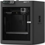
- Up to 16 Colors: Bring your designs to life with vibrant multi-color/multi-material printing capabilities, perfect for showcasing your creativity. Note: Connecting Bambu Lab AMS is required.
- 500mm/s and 20000 mm/s² Acceleration True High Speed: Don't wait around for your masterpieces. Lightning-fast printing speed lets you focus on creating, not waiting.
- Enclosed Design: Fully enclosed body improves print performance for advanced filaments. Automatic Bed Leveling: Say hello to high-quality, successful prints. Auto bed leveling makes 3D printing such an easy thing.
- Set Up in 15 Minutes: Spend more time printing and less time setting up. User-friendly design ensures a hassle-free assembly experience for all skill levels.
- Supported Filament: Ideal: PLA, PETG, TPU, PVA, PET ABS, ASA; Capable : PA, PC; Not Recommended: Carbon/Glass Fiber Reinforced Polymer.
Examples: product packaging versus transistor research
Foveros and Foveros Direct
Foveros illustrates logic-on-logic integration: Intel’s 2018 announcement describes a base die that can carry I/O, SRAM, and power delivery beneath high-performance logic chiplets. Foveros Direct illustrates a more specific interconnect approach, using copper-to-copper hybrid bonding according to Intel’s packaging overview. These are vendor descriptions of architectures and capabilities, not independent comparative performance measurements.
PC Slower Than It Used to Be?
A free scan shows the junk files, broken settings and background clutter dragging Windows down - then fixes them in one click.Free scan · Windows 10 & 11Crashes, No Sound, or Screen Glitches?
Random freezes, missing sound and display glitches usually trace back to one bad driver. Find and replace yours safely.Free scan · under a minuteTSMC SoIC
TSMC presents SoIC as wafer-level 3D integration and describes its role in bringing chiplets partitioned from a system-on-chip back together. The term identifies a platform and integration approach; it should not be treated as a synonym for every kind of chiplet or transistor stacking.
Intel Data Center GPU Max Series
Intel Foundry’s undated technology overview, accessed in 2026, says the Data Center GPU Max Series uses EMIB 3.5D and has more than 100 billion transistors, 47 active tiles, and five process nodes. Those figures describe a heterogeneous multi-die package example. They do not mean all of its transistors are vertically stacked.
Rank #4

- High-Speed Precision: The Bambu Lab P2S 3D printer prints up to 600 mm/s while maintaining exceptional accuracy. With the PMSM Servo Extruder and Active Flowrate Compensation, every layer of your printed object stays sharp and smooth, delivering flawless corners and consistent results.
- Ready to Print in 15 Minutes: Set up your P2S FDM 3D printer and start printing in just 15 minutes. With AI failure detection, quick-swap nozzles, and automatic calibration, this 3D printer makes professional-grade 3D printing effortless, even for beginners.
- Effortless Multi-Color Printing: The AMS 2 Pro enables seamless multi-color/multi-material 3D printing. It features built-in filament drying at up to 65 °C, keeping every spool ready for flawless prints. (Note: The P2S 3D printer does not support multi-color printing; Combo version required.)
- Smart Airflow for Any Filament: The Adaptive Airflow System automatically balances cooling and heat retention—keeping overhangs crisp with cool air, or maintaining a 50 °C chamber for engineering-grade materials. A carbon filter ensures clean, safe air while you print.
- Limitless Creativity, Seamless Workflow: Explore over one million 3D models on MakerWorld and bring them to life with a smooth, unified workflow using Bambu Studio, Bambu Handy, and your FDM 3D printer, from design to finished print.
Stacked transistor devices
At IEDM 2023, Intel reported a research demonstration of vertically stacked complementary field-effect transistors with gate pitch down to 60 nanometers. This is a company-reported research result about transistor architecture, distinct from a commercial chiplet package. The announcement does not establish commercial availability.
Independent reader supportYour contribution helps us test, update, and keep practical guides available for everyone.What limits 3D stacking?
Heat removal
Heat from an upper die has a more difficult path out of the stack. The IEEE’s 3D IC overview identifies thermal analysis as part of stack planning. Designers need to consider where heat-producing functions sit and how heat can escape; vertical density alone does not guarantee a workable design.
Power, interconnects, and integration
A stack must deliver power as well as signals, and its dies must be aligned and connected in a way that works for the intended design and production process. The architecture, bonding or other interconnect method, and manufacturing integration all affect whether the intended density or communication benefits are practical.
Best Value

- 600mm/s Speed & CoreXY Structure — Powered by an all-metal CoreXY frame and 20,000mm/s² acceleration, Adventurer 5M Pro reaches speeds up to 600mm/s. Integrated vibration compensation algorithms eliminate ghosting and ringing for smooth, high-precision surface finishes.
- 3-Second Quick-Swap Nozzle & Auto Leveling — Features a tool-free, quick-release nozzle mechanism for effortless 3-second replacements across multiple sizes (0.25/0.4/0.6/0.8mm). One-click full auto-leveling ensures precise bed calibration and a perfect first layer every time.
- Dual Filtration System & Quiet Enclosure — Built with an integrated dual filtration system and a fully enclosed chamber to ensure a clean printing environment and thermal stability. Powered by low-noise motion control, it operates quietly under 50dB for seamless home, office, or classroom use.
- 280°C High-Temp Extruder & Broad Material Compatibility — With a 280°C max nozzle temperature and a 110°C heated bed, it reliably prints engineering materials like ABS, ASA, and PETG-CF, as well as standard PLA and PETG.
- Smart Camera & Mobile Control — Features a built-in camera for real-time monitoring and time-lapse video creation. Monitor progress, adjust settings, and receive instant status alerts via Flash Studio. Integrated with filament detection, power loss recovery, and a 4.3-inch touchscreen for effortless operation.
No universal performance or cost figure
There is no single performance gain, energy saving, cost, or yield improvement that applies to all 3D-stacked chips. The cited vendor and engineering descriptions explain approaches and potential benefits, but do not provide an independently verified universal figure or a like-for-like benchmark across Foveros and SoIC.
How to interpret claims about a “3D chip”
When a product or technology is described as 3D-stacked, identify what is actually stacked and where integration occurs. A package may combine many dies or tiles without every die being vertically stacked; a transistor-level research structure is a different claim from a product package.
Quick Recap
- What is stacked? Separate dies or chiplets, wafers, or transistor layers?
- Where does integration happen? During package assembly, at wafer level, or during device fabrication?
- What connects the layers? Is a particular interconnect method stated, or is the description general?
- Which functions are combined? Logic, memory, I/O, cache, and power delivery have different roles.
- What evidence supports the benefit? A vendor’s design intent, a research demonstration, and an independently measured product comparison are not the same kind of evidence.
Product prices and availability are accurate as of the date/time indicated and are subject to change. Any price and availability information displayed on Amazon at the time of purchase will apply.




