What’s actually slowing this PC down?
Pick the symptom - the matching free tool is one click away.
A Wccftech report dated October 14, 2026 says a semiconductor expert used Meta’s Muse personal AI agent to design and test a cryptocurrency-focused system-on-chip (SoC) based on the RISC-V instruction-set architecture, then run software used to prepare a design for manufacturing. The reported total cost was about $2,000.
That is an ambitious engineering claim, not proof that a finished chip exists. The report does not provide a tape-out record, fabricated part, silicon measurements, or an independently reproducible throughput result for the Thru blockchain. Its “fastest on Earth” wording describes the project’s objective or claim, not a verified benchmark.
As an Amazon Associate I earn from qualifying purchases.
What the $2,000 Muse chip story actually claims
The reported experiment targeted a crypto-specific SoC for the Thru blockchain. According to Wccftech, the workflow covered chip design, testing and manufacturing-preparation software, with spending of roughly $2,000. The report presents the effort as an end-to-end demonstration of how an AI agent could assist with hardware development at a cost far below the budgets normally associated with custom silicon.
Several important details about the alleged Thru processor are not public in the available report. There is no published microarchitecture, RTL repository, tape-out documentation, silicon part number, fabrication announcement or independent benchmark. The report also does not establish how much of the work was generated by Muse, how much was written or checked by the human expert, or what hardware and software expenses make up the $2,000 figure.
#1 Best Overall

- Flexible MCU Board: Incorporate the ESP32-C3 32-bit RISC-V chip, operating up to 160 MHz, mounted multiple development ports,
- Developer Friendly: Compatible with Arduino IDE, MicroPython, CircuitPython, PlatformIO, ESP IDF, Zephyr, Matter, ESPNow, Meshtastic, WLED, ESPHome, Home Assistant, Ubidots
- Outstanding RF performance: Complete Wi-Fi functions and Bluetooth Low Energy, while supporting communication over 100m with anFL antenna
- Elaborate Power Design: 4 working modes as low as 44 μA in deep sleep mode, while supporting lithium battery charge management
- Thumb-sized Design: 21 x 17.5mm, Seeed Studio XIAO series classic form factor
What Meta says Muse can do
Meta’s official product description calls Muse “Your personal AI agent that gets things done.” The company describes a general-purpose agent that can:
- Answer questions and complete multi-step tasks.
- Browse the web and connect to applications.
- Make purchases, create images and generate documents.
- Set reminders and monitor goals while continuing work in the background.
- Build a tool when a required tool does not already exist.
Those capabilities could let an expert coordinate documentation searches, scripts, simulations and design-tool steps. Meta’s public description does not identify Muse as an electronic-design-automation (EDA) product or promise autonomous SoC development. The chip-specific account therefore comes from the Wccftech report, not from a Meta specification for a hardware-design system.
Why RISC-V is significant in this report
RISC-V is an open instruction-set architecture. It defines the instructions a processor understands, while implementers choose the core microarchitecture, memory system, peripherals, accelerators and physical-design targets. That flexibility makes RISC-V a practical starting point for a specialized processor: a team can combine a general-purpose core with cryptographic engines instead of licensing a fixed commercial CPU architecture.
Rank #2
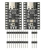
- CH32V003 Development Minimum System Board for Nano RISC-V CH32V003F4U6 Chip TYPE-C USB 22Pin
- on-board 24MHz Crystal oscillator
- Power by TYPE-C USB
In the reported project, RISC-V is the CPU architecture named for the SoC. That fact alone does not reveal the number of cores, supported extensions, clock rate, process node, memory bandwidth, security model or blockchain-specific datapath. None of those specifications has been supplied publicly for the alleged Thru chip.
How to read the available evidence
| Evidence level | What it demonstrates | What it does not demonstrate |
|---|---|---|
| RTL or generated hardware description | A circuit design can be inspected, linted and compiled for further testing. | That the design meets timing, can be manufactured or is functionally complete. |
| Simulation | Test scenarios run against a model produce the expected results under those scenarios. | Correct behavior in every workload, physical timing, power consumption or real-world throughput. |
| Place-and-route and GDS output | A physical layout database has been produced for a stated target and design flow. | Fabrication, working silicon or successful post-fabrication testing. |
| Tape-out | Manufacturing data has been formally released to a foundry. | That the wafer will work; first silicon still requires bring-up and validation. |
| Fabricated, measured silicon | A physical chip has been tested, allowing claims about speed, power and reliability under defined conditions. | Nothing beyond the tested device, configuration and workload without broader reproducibility. |
The Thru account, as reported, reaches at least the design-and-preparation stage in its description. It does not publicly establish the last two evidence levels.
What the separate museRISC project shows
A public GitHub project named museRISC provides useful context, but it is not evidence that the Thru SoC was built. Its README describes an open RV64 RISC-V processor with cryptographic acceleration and documents:
Rank #3

- The ESP32-C3 SUPERMINI is positioned as a high-performance, low-power, cost-effective IoT mini development board, suitable for low-power IoT applications and wireless wearable applications
- It is equipped with a rich set of interfaces, including 11 digital I/Os that can be used as PWM pins and 4 analog I/Os that can be used as ADC pins.
- It supports four serial interfaces, including UART, I2C, and SPI.
- The ESP32-C3 features a 32-bit RISC-V CPU, including an FPU (Floating Point Unit) capable of 32-bit single-precision
- Package: 2PCS ESP32-C3 MINI Development Board ESP32 SuperMini ESP32 C3 WiFi Module
- RTL implementations for SHA-256, SHA-512 and Keccak-f1600.
- Elliptic-curve arithmetic hardware.
- Verilator-based simulation.
- RISC-V compliance testing.
- Booting Linux 6.6 in a platform model.
- An OpenROAD-generated GDS layout for a standalone crypto macro.
The same project explicitly says the crypto macro is not attached to the processor core and that no chip has been taped out. It also warns that completing place-and-route and generating GDS do not equal fabrication or silicon verification. Those qualifications are essential: successful RTL tests and a layout file are meaningful engineering milestones, but they cannot be presented as a manufactured accelerator.
Is the Thru blockchain really “the fastest on Earth”?
There is no independently verified throughput, latency, energy-efficiency figure or test methodology in the available account. “The fastest on Earth” is wording used for the project’s stated objective in the report. A credible comparison would need a defined transaction workload, network configuration, block or confirmation rules, hardware and software versions, measurement period, and results that outside parties can reproduce.
A crypto accelerator could improve hashing, signature verification or other proof-related operations, but blockchain speed also depends on consensus, networking, storage, software implementation and economic limits. Faster arithmetic in one chip does not automatically make an entire blockchain network faster.
Rank #4

- ESP32-C6 WiFi 6 microcontroller development board adopts ESP32-C6-WROOM-1-N8 module, which is equipped with RISC-V 32-bit single-core processor, up to 160MHz main frequency, built-in 8MB Flash
- Integrates WiFi 6, Bluetooth 5 and and IEEE 802.15.4 (Zigbee 3.0 and Thread) wireless communication, with superior RF performance
- Integrates rich peripherals including SPI, UART, I2C, I2S, LED PWM, SDIO and other interfaces, compatible with the pinout of ESP32-C6-DevKitC-1-N8 development board, more convenient to use and expand a variety of peripheral modules
- Onboard CH343 and CH334 USB HUB chips, supports USB and UART development at the same time via a USB-C port
- Comes with online examples and tutorials for ESP-IDF development environment
Can an AI-assisted SoC really cost about $2,000?
The reported figure is plausible only as the budget for a particular design experiment or prototype workflow, not as a demonstrated cost for manufacturing a production chip. It may cover access to computing, software, development boards or fabrication-preparation services, but the report does not itemize the spending.
Commercial silicon normally adds expenses for EDA licensing or infrastructure, verification, intellectual-property blocks, package and board design, foundry submission, masks or shuttle fees, laboratory equipment, yield learning and multiple revision cycles. An agent can reduce time spent searching, coding and coordinating tools; it cannot remove the physical and financial requirements of fabrication and validation.
Recommended Free Tools
What would verify the claim?
- Design disclosure: Publish the SoC block diagram, ISA extensions, cryptographic datapaths, memory architecture and a versioned RTL repository.
- Reproducible verification: Provide testbenches, simulator versions, compliance logs and instructions that independent engineers can run.
- Physical-design records: Identify the process target and release the relevant timing, power, area and GDS documentation.
- Tape-out evidence: Name the foundry or shuttle program and provide a dated manufacturing release.
- Silicon results: Report the part, clock, workload, transaction rate, power, thermals and comparison baseline, with raw or independently checkable measurements.
Until those records appear, the strongest defensible description is an AI-assisted RISC-V chip-design claim reported by Wccftech, not a verified working blockchain processor.
Best Value

- Ample PSRAM Storage – The development board offers 8MB PSRAM, providing substantial extra memory for handling more complex tasks, large data buffers, and advanced processing.
- Enhanced Multi-Tasking Capability – With the additional 8MB PSRAM, the ESP32-C5-WIFI6-KIT can efficiently manage multiple protocol stacks simultaneously, ensuring smooth operation in multi-tasking IoT environments.
- Support for Medium-Load Applications – The 8MB PSRAM allows the ESP32-C5 to handle medium-load applications more effectively, making it ideal for scenarios requiring real-time data processing or continuous communication.
- Seamless Performance – The increased memory improves the overall performance and responsiveness of the device, particularly when running applications with larger memory footprints or more demanding computations.
- Future-Proof for Complex Projects – With 8MB of PSRAM, developers are better equipped to build scalable, high-performance solutions that support both current and future IoT use cases, offering flexibility for future-proofing designs.
Why the story still matters
Even without proven silicon, the experiment points to a meaningful shift in engineering workflows. General agents that can browse, write files, invoke tools and continue tasks in the background may let a small team connect specification, RTL generation, simulation and physical-design software more quickly. Open architectures such as RISC-V make that experimentation easier because the instruction set is available for implementation and extension.
The dividing line is evidence. Generated code, passing simulations and a manufacturable-looking layout are progressively stronger artifacts, but only tested silicon can support claims about real speed, efficiency and reliability. The Thru project’s $2,000 figure and “fastest on Earth” ambition should therefore be read as reported milestones and goals pending independent verification.
Quick Recap
Product prices and availability are accurate as of the date/time indicated and are subject to change. Any price and availability information displayed on Amazon at the time of purchase will apply.
Quick wins for a faster PC:
Fix the driver behind crashes, sound loss and screen glitchesFind Drivers →Repair Windows errors before they cause bigger problemsFix Now →Scan for outdated or missing drivers - takes under a minuteDriver Scan →
