Quick wins for a faster PC:
Fix the driver behind crashes, sound loss and screen glitchesFind Drivers →Clear out junk files and repair common Windows errorsFree Scan →A RAM module is the end of a long manufacturing chain, not a single part made in one step. Purified silicon is grown into a crystal, sliced into wafers, patterned and processed into many DRAM dies, electrically screened, cut apart, packaged, tested again, and finally mounted on a circuit board as a desktop UDIMM, laptop SODIMM, or another module type.
Start with the distinction: die, package and module
People often use “RAM chip” to describe several different physical objects. In manufacturing, three stages matter:
As an Amazon Associate I earn from qualifying purchases.
| Term | What it is | Where it appears in the process |
|---|---|---|
| Die | The tiny rectangular silicon circuit containing the memory cells and supporting electronics. | Created on a wafer and separated after wafer testing. |
| Package | A protective housing that connects one or more dies to external electrical contacts. | Assembled around a die that passed wafer-level screening. |
| Memory module | A circuit board carrying packaged memory devices and the contacts used by a computer. | Built after packaged parts pass their own tests; tested again as a board. |
The silicon die is where the memory circuit exists. Packaging supplies mechanical protection, environmental protection and a practical electrical interface. A module is a later board-level assembly designed for a system form factor. A desktop UDIMM and a laptop SODIMM can use related DRAM technology while differing in board dimensions, connector arrangement and system compatibility.
Recommended Free Tools
How a silicon wafer is prepared
Purify and crystallize the silicon
Manufacturing begins with silicon purified to semiconductor standards. The material is melted and formed into a single-crystal ingot. Crystal quality matters because the later transistors and capacitors must operate consistently across the wafer.
#1 Best Overall

- [Color] PCB color may vary (black or green) depending on production batch. Quality and performance remain consistent across all Timetec products.
- DDR3L / DDR3 1600MHz PC3L-12800 / PC3-12800 240-Pin Unbuffered Non-ECC 1.35V / 1.5V CL11 Dual Rank 2Rx8 based 512x8
- Module Size: 16GB KIT(2x8GB Modules) Package: 2x8GB ; JEDEC standard 1.35V, this is a dual voltage piece and can operate at 1.35V or 1.5V
- For DDR3 Desktop Compatible with Intel and AMD CPU, Not for Laptop
- Guaranteed Lifetime warranty from Purchase Date and Free technical support based on United States
Slice and polish the wafer
The ingot is cut into thin circular wafers. Slicing leaves mechanical damage and surface irregularities, so the wafers are ground, chemically treated and polished until the surface is extremely flat. The finished wafer is the shared substrate on which many copies of the eventual die will be built.
Grow an insulating oxide
An oxidation step can form a uniform silicon-oxide layer on the surface. Samsung describes this layer as helping protect the surface and reduce unwanted current leakage between circuits. Oxide is only one of the materials used in fabrication, but it illustrates why the wafer is treated as an engineered stack rather than as bare silicon.
Pattern the wafer with photolithography
Each circuit layer begins with a patterning operation. The wafer receives a light-sensitive coating called photoresist. A photomask carries the geometry for that layer, and a lithography system projects the pattern onto the resist. After exposure, the resist is developed so selected regions remain while others are removed.
The patterned resist acts as a temporary stencil. Depending on the layer, it defines where material will be deposited, etched away, implanted or otherwise modified. The wafer is then cleaned and prepared for the next operation. Advanced memory processes may use multiple patterning steps to create fine features; the exact approach depends on the manufacturer and process generation.
Alignment is critical. A new pattern must register with structures already formed underneath it. A small overlay error can change transistor dimensions, interfere with a capacitor connection or break a metal route. That is why lithography is repeated with measurement and alignment controls rather than treated as one exposure at the beginning.
Build the circuit through repeated process cycles
A DRAM wafer is made by repeating several classes of operation across many layers. The order and recipes vary by manufacturer, but the high-level jobs are consistent.
Deposition adds thin films
Deposition places controlled films on the wafer. These may be insulating, conductive or semiconducting materials. Film thickness, composition and uniformity affect the electrical behavior of every structure formed from them.
Etching removes selected material
After a layer is patterned, etching removes exposed material while leaving protected regions in place. The process must control sidewall shape, depth and selectivity so that it does not damage neighboring structures or the layers below.
Rank #2

- ✅【DDR3 8GB Kit 1333MHz UDIMM RAM 】PC3-10600, DDR3 1333MHz, Unbuffered, Dual Rank, Non ECC, 1.5V CL9, apply for AMD, Intel, Mac system
- ✅【Advanced Chips】All DDR3 8GB RAM are high quality ram memory module. Professional company, high-quality materials, upgrade designed for DDR3 UDIMM compatible desktop
- ✅【Stable and Durable】8GB DDR3-1333MHz DIMM RAM, 100% tested for stability, durability and compatibility. All PC3-10600 modules undergo quality assurance testing to ensure dependable and reliable performance
- ✅【Increases System Performance】PC3 8GB ram will speed up loading times, improve system responsiveness, and increase your system's ability to handle greater workloads. Warm tips: Please make sure your desktop model meets 2x4GB 1333 10600 kit, you can also contact us to make sure
- ✅【Lifetime Service】Lifetime warranty, free technical support. You can also contact us to ensure compatibility. Any questions, feel free to contact us, we are always be with you
Ion implantation changes electrical properties
Ion implantation introduces carefully selected dopants into silicon. The doped regions become the source, drain and other electrically active parts of transistors. Implant conditions and subsequent heat treatment determine how those regions behave.
Interconnects join the devices
Once the active devices are formed, insulating layers and patterned metal create the wiring that connects them. Modern memory uses multiple interconnect levels. Vias connect one level to another, and every level must align with the structures below it.
These operations are not a simple one-way recipe. A wafer cycles through coating, exposure, development, deposition, etch, implantation, cleaning, measurement and other steps many times. The result is a three-dimensional stack of electrical structures whose final behavior depends on the cumulative accuracy of all earlier layers.
Form the DRAM memory cell
The fundamental DRAM storage element combines a transistor with a capacitor. The transistor controls access to the capacitor, and the capacitor’s electrical charge represents the stored bit. Because charge gradually leaks away, DRAM must be refreshed while powered; that operating fact follows from the cell’s physical storage method.
Manufacturing the cell is an integration challenge. Micron’s explanation of DRAM processing describes forming transistors and tall, narrow capacitors while maintaining the alignment of successive layers. The capacitor must hold enough charge for reliable sensing, fit within the available area and connect correctly to the access transistor. Different manufacturers and generations use different layouts, materials and process details, so one company’s cell structure should not be treated as a universal recipe.
Peripheral circuits are built alongside the array. They include row and column selection, sense amplifiers, control logic and connections to the outside world. The array stores the bits, while the peripheral circuitry selects cells, detects their small electrical signals and communicates with the memory interface.
Probe the wafer before cutting it apart
A finished wafer contains many repeated die sites. Before any site is packaged, electrical die sorting—often called wafer probe—checks whether it meets the relevant functional and electrical criteria. Probe equipment contacts test structures or die pads and applies controlled signals, voltages and timing patterns.
The Tool Desk
Outbyte Driver Updater FREEFix the driver behind crashes, sound loss and screen glitchesFind Drivers →Outbyte PC Repair FREEClear out junk files and repair common Windows errorsFree Scan →Probe identifies dies that should not proceed to packaging. It also records information about performance and failure locations. Engineers use that data to monitor process stability, identify systematic defects and improve later wafer lots. The term yield means the share of die sites that meet the specified criteria; it is not a universal fixed percentage. Yield depends on the product, wafer size, process generation, test limits and production date.
Rank #3
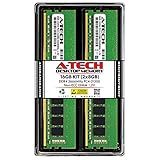
- Compatible with select DDR4 Desktop computers + Easy to install at home, no expertise required
- Maximize your system's performance, boost loading speeds and multitask with ease
- Backed by A-Tech's Lifetime Warranty + Friendly tech support team available to help before and after your purchase
- 16GB RAM Kit ( 2 x 8GB Modules ) | DDR4 DIMM 288-Pin | Speeds up to 2666MHz (2667MHz), PC4-21300 / PC4-2666V
- NON-ECC Unbuffered | 1Rx8 or 2Rx8 - Single or Dual Rank | JEDEC DDR4 standard 1.2V
Defects introduced early cannot simply be repaired at the end. Thy Tran, Micron’s vice president of DRAM Process Integration, summarizes the constraint this way: “Semiconductor fabrication isn’t like making a car. You can’t go back and fix a defect introduced earlier in the process.” Later layers can sometimes cover or isolate a problem, and process data can help detect and control recurring defects, but a failed die is normally excluded rather than rebuilt.
Singulate good dies and package them
After wafer probe, the wafer is separated into individual dies. This singulation may involve sawing, laser-based methods or another controlled separation technique, depending on the product and assembly flow. The objective is to isolate the tested die without damaging its active circuitry or connection pads.
Passing dies move into package assembly. A package attaches the die to a substrate, lead frame or another carrier, establishes electrical connections and seals the assembly against handling and the operating environment. The external package contacts are designed for the next level of use, such as a module board or a system motherboard.
Free tools Windows power users keep installed
One-click scans. No signup required.
Packaging is more than a protective cap. It must manage electrical signal paths, mechanical stress and heat while preserving the connections made to the die. Package construction also affects how many devices can fit on a module and how the finished memory can be routed by a computer designer.
Test the packaged memory device
Packaging introduces new possible failures, so a passing wafer die is not automatically a passing product. Manufacturers test packaged parts with specified voltage, signal, timing and temperature conditions. They check functional operation and electrical margins, then screen for defects that appeared during assembly.
Samsung’s published testing example includes stress or burn-in, post-burn-in checks and final tests. Burn-in applies controlled operating stress for a defined procedure; it is intended to expose parts that would fail early in service. The exact sequence, limits and duration are manufacturer- and product-specific, so this example should not be read as an identical checklist for every DRAM device.
Test results determine whether a packaged part is shipped, rejected or assigned to a specification supported by its measured behavior. The process may also sort parts by speed, density or other characteristics, but those categories and limits are product-specific rather than universal properties of all RAM chips.
Do these 3 things before closing this tab:
1Fix the driver behind crashes, sound loss and screen glitches2Clear out junk files and repair common Windows errors3Scan for outdated or missing drivers - takes under a minuteAssemble packaged chips into a RAM module
Mount the devices on a board
Packaged DRAM parts that are intended for module use are placed on a printed-circuit board. Automated assembly equipment applies solder paste or another joining material, positions each package and uses a controlled heating profile to form reliable connections. The board also carries power distribution, signal traces and the edge connector used by the computer.
Rank #4

- 【DDR3 2x 4GB 1600MHz 12800 Udimm Desktop RAM Card】DDR3-1600, PC3-12800, Unbuffered, Dual Rank, Non ECC, 2Rx8, 240-Pin, 1.5V, CL11 memoria ram
- 【Advanced Chips】All DDR3 4GB 12800 ram card are high quality ram memory module, apply for desktop computer AMD, Intel, Mac system
- 【Stable and Durable】8GB DDR3-1600MHz Udimm, 100% tested for stability, durability and compatibility. We test all rams before shipment to ensure all PC3-12800U ram card works stably and normally
- 【Increases System Performance】PC3 8GB ram will empower your computer to achieve faster loading times, system responsiveness, increase your system's ability to handle greater workloads. Note: Please make sure your desktop computer meets PC3 12800 1600 kit
- 【Lifetime Service】Compatible with Macbook, iMac, HP, Dell, Lenovo, ASUS, Acer, etc. Lifetime warranty, free technical support. Any questions, feel free to contact us, we will reply within 24hrs
Choose the module form factor
Micron identifies desktop UDIMM and laptop SODIMM as distinct module categories, along with other types. A UDIMM is sized and keyed for many desktop systems; a SODIMM is shorter for compact systems such as laptops. Form factor alone does not guarantee compatibility. The system must also support the module’s memory generation, capacity, organization, voltage and other electrical requirements.
Run module-level tests
After assembly, the complete module is tested as a system-level component. Tests check that all installed devices communicate correctly through the module’s wiring, that the board operates across specified conditions and that assembly defects have not created intermittent faults. Module testing is a separate quality gate from wafer probe and packaged-device testing.
How the stages fit together
| Stage | Primary question | Output |
|---|---|---|
| Wafer fabrication | Were the transistors, capacitors and interconnect layers formed with the required geometry and materials? | A wafer containing many patterned die sites. |
| Wafer probe | Which die sites meet electrical and functional requirements before assembly? | Known-good candidates and recorded process data. |
| Singulation and packaging | Can a passing die be separated and given durable external connections? | Individual packaged memory devices. |
| Package test | Does the assembled device meet its specified behavior under controlled conditions? | Qualified packaged parts. |
| Module assembly | Can multiple packaged parts be mounted and interconnected on the intended board? | A UDIMM, SODIMM or another module category. |
| Module test | Does the complete board function reliably as a memory component? | A tested module ready for system integration. |
Why no two DRAM manufacturing flows are exactly identical
The broad sequence—wafer preparation, patterning, device formation, probe, packaging and testing—is shared across the industry. The details are not. Manufacturers choose different materials, feature sizes, capacitor structures, lithography strategies, package designs, test limits and factory allocations. A company may also divide fabrication, assembly and testing among multiple facilities rather than completing every operation at one site.
Windows Errors? Fix Them Before They Spread
Repair common Windows errors and clear accumulated junk for a smoother, more stable PC - no reinstall needed.Free scan · no reinstallOutdated Drivers Are Slowing You Down
One free scan finds every outdated or missing driver and matches the right update for your exact hardware.Free scan · exact hardware matchProcess generations change the balance between density, speed, power consumption, manufacturing complexity and cost. A newer generation can require additional patterning or tighter alignment while using a different capacitor or interconnect scheme. Consequently, a diagram showing one manufacturer’s flow is useful for understanding the sequence, not for inferring an industry-wide step count, cycle time or yield.
What the finished module contains
By the end of the flow, the module is a coordinated assembly of packaged DRAM devices, a board, conductive traces, a connector and supporting components. The memory bits still reside in the capacitors on the silicon dies. The package makes each die usable outside the wafer, and the module makes a collection of those devices usable by a computer’s memory socket.
A desktop UDIMM is therefore not “one large RAM chip.” It is a board populated with packaged memory components arranged to meet the electrical and physical requirements of a desktop platform. A laptop SODIMM serves the same broad purpose in a smaller form factor, but its dimensions and connector layout are different. Always match the module type and electrical support specified by the target system; manufacturing category does not by itself establish compatibility.
The complete path in one view
- Purify silicon and grow a single-crystal ingot.
- Slice and polish the ingot into flat wafers.
- Form protective and functional films, including oxide where required.
- Use photolithography to pattern each layer from a photomask.
- Repeat deposition, etching, implantation, cleaning, measurement and alignment to build transistors, capacitors and interconnects.
- Probe the wafer electrically and exclude die sites that fail the required criteria.
- Separate the passing die sites from the wafer.
- Assemble each usable die into a protective, electrically connected package.
- Test the packaged parts under specified operating and stress conditions.
- Mount selected packaged parts on a module board such as a UDIMM or SODIMM.
- Test the completed module for function and reliability before system installation.
The important boundary is between the silicon circuit and the products built around it: wafer fabrication creates dies, packaging turns dies into usable chips, and module assembly turns those chips into the removable memory boards found in computers.
Quick Recap
Product prices and availability are accurate as of the date/time indicated and are subject to change. Any price and availability information displayed on Amazon at the time of purchase will apply.

