PC Slower Than It Used to Be?
A free scan shows the junk files, broken settings and background clutter dragging Windows down - then fixes them in one click.Free scan · Windows 10 & 11Outdated Drivers Are Slowing You Down
One free scan finds every outdated or missing driver and matches the right update for your exact hardware.Free scan · exact hardware matchCommon-mode noise in a differential transmission occurs when both conductors in a pair move together in the same direction relative to a reference, such as chassis, ground, or a nearby return structure. Unlike the intended differential signal, which is defined by the voltage difference between the two conductors, common-mode energy is the shared component that ideally remains small but often appears due to real-world imbalance in drivers, routing, interconnects, return paths, and terminations.
This unwanted shared voltage or current can degrade signal integrity, reduce receiver margin, and convert efficiently into radiated or conducted electromagnetic interference. Even when a receiver rejects much of the common-mode component, excessive common-mode noise can stress input limits, increase jitter through mode conversion, and make a design fail emissions or immunity requirements.
Understanding common-mode noise requires looking at both the electrical behavior of the differential pair and the physical implementation around it. PCB geometry, cable construction, connector transitions, skew, impedance mismatch, ground discontinuities, and measurement setup all influence how common-mode noise is created, observed, and controlled.
What Common-Mode Noise Means in Differential Transmissions
In a differential transmission, two conductors carry signals that are intended to be equal in magnitude and opposite in polarity. The receiver ideally responds only to the voltage difference between the two lines, such as Vdiff = V+ – V–. Common-mode noise is the portion of unwanted voltage or current that appears in the same direction on both conductors at the same time. Instead of one line moving up while the other moves down, both lines shift together relative to a reference such as chassis, cable shield, PCB ground, or earth.
Free tools Windows power users keep installed
One-click scans. No signup required.
#1 Best Overall

- Shortwave Choke Magnetic Ring: Specifically designed for high frequency radios operating between 1.8 to 30MHz, it effectively suppresses common mode currents and eliminates electromagnetic interference.
- Powerful: This high magnetic permeability ferrite magnetic ring bears high temperatures and saturation, supporting high power applications without compromising performance.
- Plug and Play: Featuring an M male to M female connector, the installation of the shortwave choke magnetic ring is quick and labor saving. Simply plug it in to start using it immediately.
- Versatile Applications: This magnetic ring is suitable for various scenarios including shortwave communication, radio frequency testing, and emergency communications.
- Specifications: The EM43 magnetic ring has a diameter of 45mm and a power capacity of 150W PEP, ensuring that your communication signals remain pure and undisturbed.
A useful way to visualize it is to separate the pair voltage into two parts: the differential component, which carries the intended data, and the common-mode component, which represents the average voltage of the two conductors. In simplified form, the common-mode voltage is VCM = (V+ + V–) / 2. If a pair swings from 1.2 V to 0.8 V on one line while the other swings from 0.8 V to 1.2 V, the average stays at 1.0 V and the common-mode level is stable. If both lines are simultaneously shifted upward by 100 mV because of ground bounce or coupled interference, that 100 mV shift is common-mode noise.
Common-mode noise differs from differential-mode noise because of how it appears to the receiver and how it returns through the interconnect. Differential-mode noise changes the voltage difference between the two conductors and directly corrupts the data eye, timing threshold, or analog amplitude. Common-mode noise ideally cancels at a perfectly balanced differential receiver, but real systems are never perfectly balanced. Input impedance mismatch, skew, unequal parasitic capacitance, connector asymmetry, bends, vias, and cable imbalance can convert part of the common-mode energy into differential noise that the receiver does see.
The electrical behavior of common-mode noise also matters because its return path is not confined to the tight loop formed by the two traces. Common-mode current tends to return through nearby reference planes, chassis structures, cable shields, stray capacitance, and any available conductive path. This larger return geometry can make the interconnect behave like an antenna, especially when the cable or trace structure becomes a significant fraction of a wavelength at the noise frequency. For this reason, a system may pass functional tests while still producing excessive radiated emissions.
Common forms in practical differential links
- Common-mode voltage offset: a DC or low-frequency shift of both lines due to ground potential differences, bias network errors, or transceiver output imbalance.
- Common-mode ripple: periodic noise coupled from switching regulators, clocks, motor drives, or digital return currents into both conductors.
- Common-mode current: current flowing in the same direction on both conductors, often associated with radiation from cables, connectors, and board edges.
- Mode-converted noise: common-mode energy transformed into differential-mode disturbance by discontinuities or imbalance in the channel.
Common-mode noise is therefore not just an abstract measurement term. It links signal integrity, electromagnetic compatibility, and receiver robustness. A high-speed serial link, an LVDS clock, a USB pair, an Ethernet cable, or an RS-485 bus may all tolerate some common-mode movement, but only within the input common-mode range and noise rejection capability of the receiver. Once the common-mode level exceeds that range, or once imbalance converts it into differential error, the result can be increased jitter, eye closure, bit errors, intermittent communication failures, or failed EMI compliance tests.
Common-Mode vs. Differential-Mode Signals
In a differential link, the receiver is primarily interested in the voltage difference between the two conductors. If the positive conductor is at 600 mV and the negative conductor is at 200 mV, the differential-mode voltage is 400 mV. If both conductors move upward or downward together by the same amount, that shared movement is common-mode voltage. Mathematically, differential-mode voltage is usually expressed as Vdiff = Vp − Vn, while common-mode voltage is Vcm = (Vp + Vn) / 2.
The distinction matters because these two signal components behave very differently. Differential-mode energy is the intended signaling energy in interfaces such as USB, Ethernet, LVDS, CAN, PCIe, and many SERDES links. It flows as equal and opposite currents in the pair, so the fields tend to cancel in the surrounding space when the geometry is well balanced. Common-mode energy, by contrast, appears in phase on both conductors relative to a reference such as chassis, cable shield, or PCB ground. Because the two currents are not canceling each other in the same way, common-mode current can excite cables, connector structures, heatsinks, and board planes as antennas.
| Aspect | Differential mode | Common mode |
|---|---|---|
| Voltage definition | Difference between the two conductors | Average voltage of both conductors relative to a reference |
| Current direction | Equal and opposite currents | Currents largely in the same direction relative to the return environment |
| Desired in data links | Yes, it carries the information | Usually no, except for defined bias or termination conditions |
| Radiation tendency | Low when the pair is tightly coupled and balanced | Often much higher, especially on cables and connectors |
A real waveform usually contains both components at the same time. For example, a driver may launch a clean 800 mV differential signal, but skew between the two legs, unequal rise times, or asymmetric impedance can convert part of that energy into common-mode noise. The reverse can also occur: common-mode disturbances from power-supply noise, ground bounce, or external interference can be converted into differential-mode noise if the receiver input, interconnect, or termination is not well balanced. This mode conversion is a central signal-integrity concern because receivers reject common-mode voltage only within finite limits.
Differential receivers are specified with a common-mode input range and a common-mode rejection ratio. As long as the shared voltage on the pair stays within the allowed range and remains sufficiently rejected, the receiver can recover the intended differential signal. If common-mode voltage is too large, too fast, or converted into differential noise, it can reduce eye height, shift crossing points, increase jitter, or cause bit errors. Even when the link still functions, common-mode current may create electromagnetic interference problems that show up during radiated-emissions testing, particularly when a balanced pair exits the PCB through a connector into a long cable.
Rank #2

- INDUSTRIAL GRADE ANTI INTERFERENCE: This device is designed for 1.8-30MHz high frequency radio stations, eliminating noise wave for pure signal.
- COMMON MODE CURRENT SUPPRESSION: Efficiently eliminates electromagnetic interference EMI, ensuring clean comm signals during outdoor operations and competitions.
- FERRITE RING: Constructed with high permeability ferrite magnetic rings, the EM25 boasts anti high temperature and antisaturation, ensuring no magnetic degradation even under high power usage.
- LIGHTWEIGHT AND PORTABLE: Compact with a diameter of 25mm and fast heat dissipation, the EM25 shortwave choke magnetic ring supports up to 100W PEP.
- PLUG AND PLAY: Featuring an M male (PL 259) to M female (SO 239) connector, this magnetic ring allows for quick and efficient installation, easily connecting your radio and feedlines in just 3 seconds.
For analysis and debugging, separating the two modes is often more useful than looking at each conductor individually. Two single-ended oscilloscope probes may show that both traces are noisy, but calculating Vdiff and Vcm reveals whether the noise directly corrupts the data or mainly represents shared motion of the pair. This separation helps determine whether the best fix is tighter length matching, improved return-path continuity, better connector symmetry, common-mode choking, termination changes, or reduced coupling from nearby aggressors.
Key Characteristics of Common-Mode Noise
Common-mode noise on a differential pair is the voltage component that appears in the same polarity on both conductors with respect to a reference such as chassis, cable shield, or circuit ground. If the two line voltages are VP and VN, the common-mode voltage is typically expressed as (VP + VN) / 2, while the useful differential signal is VP – VN. In an ideal differential channel, the receiver ignores the common component. In real systems, imbalance in the driver, interconnect, return path, connector, cable, or receiver converts some of that common-mode energy into differential error and some into radiated or conducted emissions.
A defining characteristic of common-mode noise is that its return current does not simply flow as an equal and opposite current tightly coupled to the adjacent trace. Instead, common-mode current may return through planes, chassis, shields, parasitic capacitance, cable braids, heatsinks, enclosure seams, or external equipment. This often creates a much larger current loop than the differential current path. Because radiation increases with loop area and cable length, even a small common-mode current can dominate electromagnetic emissions, especially when it excites a cable or enclosure structure near resonance.
Electrical traits commonly seen in differential links
- Same-polarity voltage on both conductors: both members of the pair move up or down together relative to the local reference.
- Frequency-dependent behavior: common-mode content is often strongest at signal edges, clock harmonics, switching-regulator frequencies, and resonances in cables or enclosures.
- Mode conversion: discontinuities and asymmetry can convert differential energy into common-mode energy, and common-mode energy back into differential noise at the receiver.
- Reference sensitivity: measured amplitude depends on where the reference is taken, such as board ground, chassis, shield, or a remote instrument ground.
- Poor correlation with eye height alone: a link may show an acceptable differential eye diagram while still producing excessive common-mode EMI.
Common-mode noise also has a strong relationship with balance. A perfectly symmetrical pair driven by equal and opposite signals has very little common-mode output, but practical designs always include tolerances. Trace width and spacing variation, skew between the two conductors, different via structures, uneven solder pads, connector pin-field asymmetry, nonuniform cable twist, and unequal loading all disturb the balance. The disturbance may be small in voltage terms, but at multi-gigabit edge rates it can produce substantial high-frequency spectral content.
Another characteristic is that common-mode noise is often intermittent or layout-dependent rather than purely source-dependent. For example, the same serializer may pass emissions testing on one board and fail on another because of a split reference plane under the pair, an asymmetric ESD device, or a connector transition that changes the common-mode impedance. Similarly, a cable assembly can change results dramatically depending on shield termination, pair twist quality, drain-wire placement, and how the cable is routed near metalwork.
From a receiver perspective, common-mode noise is constrained by the input common-mode range and the receiver’s common-mode rejection ratio. If the common-mode voltage moves outside the allowed range, the input stage can lose linearity, increase jitter, or make bit decisions incorrectly. Even within the allowed range, finite rejection means some common-mode disturbance can appear as differential noise, reducing timing margin and increasing deterministic jitter. For this reason, common-mode noise is both an EMI concern and a signal-integrity concern, particularly in high-speed serial links, long cables, and systems with mulle ground domains.
Major Causes of Common-Mode Noise
Common-mode noise in a differential link usually appears when the two conductors stop behaving as a perfectly balanced pair. In an ideal differential channel, equal and opposite currents flow in the two traces or wires, so their external fields largely cancel and the receiver responds only to the voltage difference. Real PCB and cable systems introduce asymmetry, discontinuities, and coupling paths that convert part of the intended differential signal into common-mode voltage or current.
Imbalance in the differential pair
The most common source is mismatch between the positive and negative sides of the channel. If one trace is longer, wider, closer to a reference plane, or routed through a different dielectric environment than the other, the two signals no longer arrive with identical amplitude and timing. This skew and impedance mismatch create mode conversion. Even small asymmetries can matter at multi-gigabit data rates because fast edges contain high-frequency energy that is sensitive to tiny geometry differences.
What’s actually slowing this PC down?
Pick the symptom - the matching free tool is one click away.
Rank #3

- HELPS SUPPRESS COMMON-MODE RF CURRENT Designed to help suppress unwanted common-mode RF current commonly found in end-fed and other unbalanced antenna systems, helping reduce RF energy traveling on the outside of the coaxial feed line.
- HELPS REDUCE RF FEEDBACK May help reduce RF feedback and feed-line radiation that can affect compatible radio equipment. Actual performance depends on the antenna system, installation, and operating conditions.
- HIGH-PERFORMANCE FERRITE DESIGN Constructed with a high-performance ferrite sleeve optimized for HF and VHF frequency ranges, providing broadband common-mode suppression in a compact inline design.
- COMPACT AND EASY TO INSTALL Small, lightweight inline design installs easily at the antenna feed point, antenna tuner, transceiver, or other suitable locations along the coaxial feed line.
- FOR AMATEUR RADIO ANTENNA SYSTEMS Suitable for end-fed antennas, HF/VHF mobile radio systems, portable stations, field operation, emergency communication, and other compatible amateur radio antenna systems.
- Length mismatch: different propagation delays cause one side of the pair to switch slightly earlier than the other.
- Impedance mismatch: unequal trace width, spacing, or dielectric loading changes the voltage-current relationship on each conductor.
- Unequal loss: one polarity may experience more attenuation due to copper roughness, vias, connectors, or nearby structures.
- Routing asymmetry: one trace passing near a split plane, void, via field, shield contact, or noisy component can pick up extra disturbance.
Discontinuities from vias, connectors, and transitions
Every transition in a differential channel can disturb balance. Vias add inductance and capacitance, and if the two vias are not placed symmetrically with nearby return paths, they can generate common-mode current. Connectors, sockets, mezzanine interfaces, and package breakouts are also frequent contributors because pin fields rarely preserve the same coupling and reference geometry as a tightly routed PCB pair. Cable-to-board transitions are especially sensitive, since shield termination, pin assignment, and connector launch geometry determine whether return current stays controlled or spreads into the chassis and surrounding conductors.
Reference-plane and return-path problems
Differential signals still interact with reference planes, especially when pair spacing is not extremely tight or edge rates are high. If a pair crosses a split plane, changes layers without nearby stitching vias, or passes over an aperture in the reference structure, the return current path becomes disrupted. The resulting field imbalance can excite common-mode current on the pair, nearby copper, connector shells, or cable shields. Poor plane stitching between PCB regions, weak chassis bonding, and long return loops can make this effect worse by giving common-mode current a larger structure to radiate from.
External coupling and power-related noise
Common-mode noise can also be injected from outside the differential pair. Switching regulators, clock traces, memory buses, motor drives, RF transmitters, and ESD events can capacitively or inductively couple into both conductors at the same time. Power supply noise may enter through transmitter or receiver ground bounce, imperfect on-die termination, or package parasitics. When the local ground reference at the driver differs from the receiver reference, that voltage difference can appear as common-mode stress across the interconnect.
| Cause | Typical mechanism | Common result |
|---|---|---|
| Trace skew | Unequal delay between conductors | Differential-to-common-mode conversion |
| Via or connector imbalance | Asymmetric parasitic capacitance and inductance | Reflections and radiated emissions |
| Reference-plane discontinuity | Interrupted return current path | Common-mode current on planes, shields, or cables |
| External noise coupling | Shared electric or magnetic field pickup | Receiver margin loss and EMI failures |
In practice, several of these mechanisms often combine. A slightly skewed pair may pass through an imperfect connector, then attach to a cable with a poorly bonded shield, creating enough common-mode current to cause EMI problems even when the differential eye diagram looks acceptable. This is controlling symmetry, return paths, launch design, and nearby noise sources is central to robust differential transmission design.
Recommended Free Tools
How Common-Mode Noise Affects Signal Integrity and EMI
Common-mode noise is not always visible in the differential eye diagram at first glance, but it can still create serious signal integrity and electromagnetic compatibility problems. In an ideal differential link, the receiver responds only to the voltage difference between the positive and negative conductors. Real receivers, connectors, packages, vias, cables, and PCB return paths are imperfect, so some common-mode energy can convert into differential-mode noise. Once that happens, the unwanted voltage directly subtracts from timing and voltage margin at the receiver.
One common signal integrity effect is eye closure. Common-mode disturbances can couple through finite common-mode rejection in the receiver input stage, especially at high frequency where device balance degrades. The result may appear as added jitter, vertical noise, duty-cycle distortion, or intermittent bit errors. In serial links such as USB, PCIe, Ethernet, HDMI, or LVDS-based interfaces, the problem often becomes worse around discontinuities: connector transitions, AC-coupling capacitors, via fields, skewed pair routing, or cable exits. These structures can convert a portion of the common-mode voltage into differential error because each side of the pair no longer sees exactly the same impedance and delay.
Common-mode current is also a major EMI source. Differential currents are largely contained between the two conductors because their fields cancel when the pair is tightly coupled and balanced. Common-mode current, however, flows in the same direction on both conductors and returns through parasitic paths such as chassis, cable shields, reference planes, heatsinks, or free space. This creates a much larger current loop or antenna structure. A cable attached to a noisy interface can therefore radiate efficiently even when the differential signal itself is within specification.
Typical system-level impacts
- Reduced receiver margin: finite common-mode rejection allows part of the noise to appear as differential input error.
- Increased jitter: common-mode disturbances can shift input threshold crossings and degrade timing margin.
- Mode conversion: impedance imbalance changes common-mode energy into differential-mode noise, especially at connectors, vias, and cable transitions.
- Radiated emissions: common-mode current on cables and board structures can exceed EMI limits even when the data eye looks acceptable.
- Susceptibility problems: external RF fields can induce common-mode voltage that later converts into differential noise inside the product.
The EMI impact is often disproportionate to the measured voltage. A few millivolts of common-mode voltage can drive enough current onto a long cable to fail radiated emissions testing. The effective antenna length, shield termination quality, enclosure bonding, and return-path continuity all influence how much energy is radiated. This is products may pass bench-level functional testing but fail compliance testing in a chamber: the receiver may tolerate the noise, while the attached cable radiates it efficiently.
Rank #4
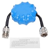
- Common Mode Suppression: Shortwave Choke Magnetic Ring effectively blocks common mode currents across the 1.8-30MHz spectrum, eliminating RF interference to ensure clear communication signals during ham radio operations.
- High Power Handling: This 1:1 current balun supports up to 100W PEP (EM25 model) with a 200W withstand power, utilizing high permeability ferrite that resists saturation and maintains stable impedance under high temperature conditions.
- Plug and Play Setup: Equipped with an integrated M male to M female connector, this HF choke coil installs directly inline without extra cables or soldering, saving setup time for field and base station use.
- Compact & Rugged Build: Featuring a 45mm diameter magnetic ring, this common mode choke fits portable radio kits while delivering lasting mechanical stability in harsh outdoor ham environments.
- Broad Frequency Consistency: Maintains uniform suppression performance from 1.8MHz through 30MHz, making it suitable for multi-band HF operations including contesting, DXing, and emergency communication scenarios.
Common-mode noise also affects interoperability. A transmitter with excessive output imbalance may work with a tolerant receiver on a short internal trace, then fail with a different cable, connector, or device at the far end. Similarly, a receiver with poor common-mode rejection may be sensitive to ground offsets, power supply noise, or coupled switching noise from nearby converters and clocks. The link may show pattern-dependent errors, temperature sensitivity, or failures only in certain mechanical configurations because the common-mode return path changes with cable placement and chassis contact.
Reducing these effects requires controlling both conversion and radiation paths. Maintaining tight pair symmetry, continuous reference planes, matched lengths, balanced via structures, and clean connector breakouts helps prevent common-mode energy from becoming differential noise. Proper cable shield bonding, common-mode chokes where appropriate, careful return-path design, and filtering at noisy boundaries reduce the amount of common-mode current that can escape the PCB. The best results come from treating common-mode noise as both a signal integrity issue and an EMI issue, rather than as a problem isolated to one discipline.
Independent reader supportYour contribution helps us test, update, and keep practical guides available for everyone.Measuring and Diagnosing Common-Mode Noise
Measuring common-mode noise in a differential link means looking at the portion of the two conductor voltages that moves together with respect to a reference plane, chassis, or local circuit ground. For a pair with single-ended voltages Vp and Vn, the differential component is typically viewed as Vp − Vn, while the common-mode component is (Vp + Vn) / 2. In practice, the measurement setup must preserve the balance of the pair; otherwise, the probe, fixture, or cable can create the very mode conversion being investigated.
A high-bandwidth oscilloscope with two matched channels is a common starting point. Probe the positive and negative conductors at the same physical location, use identical probes or matched coaxial connections, and apply math functions to calculate differential and common-mode waveforms. Channel skew should be deskewed, because even a few picoseconds of timing mismatch can make a fast differential edge appear to have excess common-mode energy. Probe loading also matters: unequal capacitance or ground lead inductance on one side of the pair can unbalance the line and distort the result.
The Tool Desk
Outbyte Driver Updater FREEFix the driver behind crashes, sound loss and screen glitchesFind Drivers →Outbyte PC Repair FREERepair Windows errors before they cause bigger problemsFix Now →Common measurement methods
- Two-channel oscilloscope math: Captures Vp and Vn separately, then derives (Vp + Vn) / 2. This is useful for time-domain debugging of edge-related noise, skew, ringing, and periodic disturbances.
- Differential probes with common-mode visibility: Some active probes provide high common-mode rejection for differential viewing, but that same rejection can hide common-mode content. Use the probe mode and specifications carefully.
- Common-mode current probes: A clamp-on RF current probe around both conductors of a cable or pair measures current flowing in the same direction on both wires. This is especially useful for EMI troubleshooting.
- Vector network analyzer measurements: Mixed-mode S-parameters can show differential-to-common-mode conversion, such as Scd21 or Sdc21, across frequency.
- Near-field probing: Magnetic and electric near-field probes can locate areas where common-mode current is coupling into shields, chassis seams, connectors, or reference-plane discontinuities.
Diagnosis usually starts by separating source, path, and victim. If common-mode voltage appears near the transmitter, check output skew, rise/fall mismatch, package escape routing, and termination balance. If it grows after a connector, cable, or via field, look for asymmetry, pinout imbalance, shield termination issues, or reference-plane interruptions. If emissions peak at cable resonances, the cable may be acting as an antenna driven by common-mode current rather than by the intended differential signal.
| Observation | Likely area to inspect |
|---|---|
| Common-mode spikes aligned with signal edges | Driver skew, routing length mismatch, via imbalance, return-path discontinuity |
| Strong noise at a switching-regulator frequency | Power rail coupling, ground bounce, poor decoupling, shared return impedance |
| Emissions increase when a cable is attached | Shield bonding, connector transition, cable balance, chassis return path |
| Common-mode level changes with board flex or cable position | Mechanical connector contact, shield termination, uncontrolled cable routing |
Practical reduction work should be verified with before-and-after measurements, not only with layout assumptions. Shorten and symmetrize breakout regions, keep both conductors over the same continuous reference plane, match via structures, and place terminations so each side of the pair sees the same impedance. Where cable radiation is the dominant symptom, common-mode chokes, improved shield bonding, or connector pinout changes may reduce current without degrading the desired differential signal. For compliance-oriented work, correlate bench measurements with chamber scans so the measured common-mode component is tied to actual radiated or conducted emissions.
Design Practices That Reduce Common-Mode Noise
Reducing common-mode noise starts with keeping the two conductors in a differential pair as electrically identical as possible. Any imbalance in impedance, propagation delay, return path, coupling, or termination can convert part of the intended differential signal into common-mode energy. Good layout practice therefore focuses on symmetry from the transmitter pins to the receiver pins, including vias, connectors, cables, and any protection or filtering components placed in the path.
PCB layout practices
- Route the pair together with consistent spacing: Keep the positive and negative traces adjacent and parallel so they experience the same dielectric, reference plane, and nearby aggressors. Avoid spreading the pair apart except where absolutely required for pin escape.
- Control differential and single-ended impedance: Meeting only the differential impedance target is not always enough. Large single-ended impedance differences between the two traces can increase mode conversion, especially at high edge rates.
- Match electrical length where it matters: Intra-pair skew causes one side of the pair to switch earlier than the other, creating a temporary common-mode voltage. Match lengths near discontinuities and across the full route based on the interface timing and rise-time requirements.
- Maintain a continuous return path: Route over a solid reference plane and avoid crossing plane splits, voids, or gaps. If a layer transition is unavoidable, place nearby stitching vias so return current can transfer cleanly between reference planes.
- Minimize asymmetric discontinuities: Use balanced via structures, similar pad shapes, and symmetric breakouts. If one trace requires a via, the other often should use a matching via to preserve balance, even if the second via is only for symmetry.
Component placement also has a strong effect on common-mode behavior. AC-coupling capacitors should be placed symmetrically, with equal pad geometry and equal trace length into and out of each capacitor. ESD diodes, common-mode chokes, connectors, and test points should be selected and placed so their parasitic capacitance and inductance are well matched on both lines. A protection device with unequal capacitance to ground can create measurable common-mode conversion at multi-gigabit data rates.
Best Value

- Common Mode Filter – Helps reduce common-mode current across 1.3–500 MHz antenna systems.
- High Power Rating – Supports up to 1500 W maximum input power for compatible installations.
- Low Insertion Loss – Designed with insertion loss below 0.4 dB within the specified operating range.
- SO-239 Connectors – Standard UHF connectors provide convenient integration with compatible coaxial systems.
- Durable Construction – Built for amateur radio base stations, portable operation, and fixed antenna installations.
Cable, connector, and termination practices
For cable-based links, preserve pair balance through the connector pinout and cable assembly. Assign the two conductors of each pair to adjacent, geometrically matched connector pins, and avoid routing one side of the pair near chassis, shields, or noisy power pins more than the other. Shield termination should be intentional: poor shield bonding or long pigtails can increase common-mode current on the cable shield. In many high-speed systems, low-impedance 360-degree shield termination to chassis near the connector gives better high-frequency performance than a long wire connection.
| Design area | Practice | Common-mode benefit |
|---|---|---|
| Pair routing | Keep spacing, width, and environment consistent | Reduces imbalance and mode conversion |
| Layer transitions | Use symmetric vias and nearby stitching vias | Provides a cleaner return path and less radiation |
| Terminations | Match termination values and placement | Prevents unequal loading of the two conductors |
| Connectors and cables | Maintain balanced pinout and shield bonding | Limits common-mode current on external structures |
Filtering can help, but it should not be used as a substitute for balanced design. A common-mode choke can attenuate common-mode current while passing the differential signal, making it useful near external connectors for interfaces such as USB, Ethernet, LVDS, CAN, or HDMI. The choke must be chosen for adequate differential bandwidth, low mode conversion, suitable current rating, and stable impedance over the noise frequency range of concern. Poorly chosen chokes can distort edges, increase jitter, or create resonances with cable and connector parasitics.
Terminations should be accurate and symmetrical. Differential termination at the receiver reduces reflections, while any biasing or failsafe network must load both conductors evenly. In mixed-signal or noisy power environments, isolate differential routes from switching regulators, clock nodes, and high-current return paths. Finally, verify the result with measurements: check common-mode voltage or current with a high-bandwidth differential setup, current probe, or mixed-mode S-parameters, then correlate findings with eye diagrams and EMI scans. The most effective reduction usually comes from combining balanced geometry, clean return paths, symmetric components, and controlled cable-to-chassis transitions.
Frequently Asked Questions
How can I tell if a differential pair problem is common-mode noise or differential-mode noise?
Measure both conductors with respect to the same reference, then calculate the average and difference of the two voltages. Differential-mode noise appears as an unwanted voltage between the two lines, while common-mode noise appears nearly the same on both lines at the same time. If the receiver eye looks acceptable but emissions are high, common-mode noise is often a strong suspect.
Do these 3 things before closing this tab:
1Repair Windows errors before they cause bigger problems2Scan for outdated or missing drivers - takes under a minute3Clear out junk files and repair common Windows errorsCan common-mode noise still matter if the differential receiver rejects it?
Yes. Receivers have limited common-mode rejection, and that rejection usually gets worse at higher frequencies. Excess common-mode voltage can also push the input outside its allowed common-mode range, increase jitter through mode conversion, or create EMI even when the receiver still seems to decode data correctly.
What PCB layout mistakes most often create common-mode noise on differential pairs?
Common causes include unequal trace lengths, asymmetric routing, crossing plane splits, poor return-path continuity, and placing one trace closer to aggressors or reference-plane changes than the other. Via imbalance and connector pinout asymmetry can also convert part of the intended differential signal into common-mode energy. Keeping the pair tightly coupled and geometrically balanced helps reduce this conversion.
How do cables and connectors contribute to common-mode noise?
Cables can radiate common-mode current efficiently because the cable shield or pair can act like an antenna. Skew between conductors, imperfect shield termination, unbalanced connector geometry, and ground potential differences between boards can all increase common-mode current. This is especially common in high-speed links that leave the PCB, such as USB, Ethernet, HDMI, LVDS, and SerDes connections.
What are the most practical ways to reduce common-mode noise in a design?
Start with balanced differential routing, continuous reference planes, matched vias, and symmetric connector transitions. Add common-mode chokes where appropriate, especially near cable exits, but verify that they do not degrade the desired differential signal. Good return-path control, proper shield termination, and avoiding ground discontinuities often reduce both EMI and receiver stress.
Quick wins for a faster PC:
Repair Windows errors before they cause bigger problemsFix Now →Scan for outdated or missing drivers - takes under a minuteDriver Scan →Bottom Line
Common-mode noise is the unwanted voltage or current that appears in phase on both conductors of a differential pair, and it matters because it can reduce receiver margin, convert into differential noise, and drive EMI from cables, connectors, and PCB structures. Even when the differential signal looks acceptable, imbalance in routing, return paths, terminations, or coupling can create common-mode energy that compromises real-world performance.
The next step is to treat common-mode control as part of the full interconnect design: keep the pair balanced, preserve continuous return paths, match terminations, avoid asymmetric coupling, and verify with the right probing or current-measurement methods. If emissions or link margin are still problematic, use targeted fixes such as layout corrections, common-mode chokes, filtering, or improved grounding and shielding.
Quick Recap
Product prices and availability are accurate as of the date/time indicated and are subject to change. Any price and availability information displayed on Amazon at the time of purchase will apply.



