Recommended Free Tools
Some links on this page are affiliate links: if you buy through them we may earn a commission, at no extra cost to you.
Mears Silicon Technology (MST) is Atomera’s engineered-materials approach to changing how silicon devices behave, with the aim of improving performance, power use, leakage and variability without relying only on a costly move to a smaller process node. The proposition is technically interesting, but its value depends on device-specific results and successful customer integration—not on a universal “full-node” gain.
That distinction is useful context for EE Times’ PowerUp podcast, “Unlocking Semiconductor Efficiency with MST Technology”. Published November 27, 2024, the 21-minute, 4-second Episode 12 features host Maurizio Di Paolo Emilio and guest Shawn Thomas, whom EE Times identifies as Atomera’s head of advanced logic nodes and power business. This explainer unpacks the technology behind the discussion, what Atomera reports, and what semiconductor customers would still need to verify.
What MST is—and what it is not
MST stands for Mears Silicon Technology. Atomera describes it as a material-layer technology: extremely thin layers of a non-semiconductor material, such as oxygen, are introduced into silicon while preserving epitaxial growth. The goal is to alter material and device behavior within a semiconductor structure. MST is not a complete transistor architecture, a software optimization, or a new bulk semiconductor such as gallium nitride (GaN) or silicon carbide (SiC).
Quick wins for a faster PC:
Fix the driver behind crashes, sound loss and screen glitchesFind Drivers →Clear out junk files and repair common Windows errorsFree Scan →The intended effects include controlling dopant movement and profiles, influencing carrier mobility, reducing unwanted leakage, and limiting device-to-device variation. Atomera calls its platform “quantum-engineered”; for evaluating it, the practical questions are what structure is added, how it changes device behavior, and whether those changes survive manufacturing and product qualification. See the company’s descriptions of MST’s material approach and its broader technology proposition.
#1 Best Overall
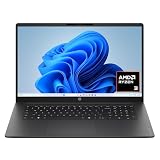
- FULL HD IPS DISPLAY - Enjoy vibrant, crystal-clear images with 178-degree wide-viewing angles
- AMD RYZEN 3 30 PROCESSOR - Everyday performance you can count on; Multitask, stream, game casually, and edit photos smoothly with responsive power and vibrant HDR visuals
- ENJOY UP TO 14 HOURS AND 15 MINUTES OF BATTERY LIFE - HP Fast Charge restores battery from 0 to 50% in approximately 45 minutes
- AMD RADEON 610M GRAPHICS - Experience smooth entertainment; Built for streaming and multitasking, enjoy realistic visuals and efficient performance for work and play
- STORAGE AND MEMORY - 512 GB PCIe NVMe M.2 SSD offers fast speed and efficient storage; and 8 GB LPDDR5 RAM memory boosts performance with higher bandwidth
Why semiconductor makers care about efficiency
“Efficiency” can mean several different things in chip manufacturing. A transistor that delivers more current may improve speed, but speed alone is not energy efficiency. Lower leakage can reduce static power, while better drive at a given voltage may improve performance per watt. Better consistency can help designers meet specifications with fewer weak devices, potentially improving yield. In power electronics, the relevant measures may instead include breakdown voltage, on-resistance, gate charge and switching loss.
These objectives are increasingly difficult to optimize together. Scaling to a new node can bring performance and density gains, but it also brings redesign, qualification, process-control and capital challenges. Mature process nodes remain useful for many analog, power and embedded products, yet manufacturers may want more capability from them. Atomera’s core pitch is to improve a process by engineering material properties rather than depending exclusively on geometric scaling.
How MST could affect device performance
Dopant profiles and mobility
Dopant atoms set important electrical characteristics in silicon devices, but heat and subsequent process steps can cause dopants to diffuse from their intended locations. Atomera says MST can help control diffusion and shape dopant profiles. That may support changes in device behavior, including improved carrier mobility or drive current, depending on the device and integration recipe.
Atomera reports that third-party evaluations have demonstrated drive-current increases of 10%–20% and mobility improvements. These are company-reported evaluation results, not a guarantee for every transistor, process node or product. A customer would need to know the baseline device, measurement method, process conditions and statistical spread before using the figures in a design or business case.
Leakage and power
Leakage is current that flows when a device is meant to be off. Reducing it can lower static power, particularly in products that spend substantial time idle. Atomera reports gate-leakage reductions greater than 60% in third-party evaluations. That figure should not be read as a 60% reduction in total chip power: chip power also includes switching activity, interconnect, memory, clocking and other circuits. Nor does a gate-leakage result automatically predict the benefit in a different device or process.
In some designs, improved drive or leakage characteristics could let engineers meet a performance target at a lower voltage, reducing energy per operation. That outcome requires circuit-level evaluation. Increased drive current can carry trade-offs, and an isolated transistor improvement does not establish a system-level power saving.
Rank #2

- Intel Celeron N4120: 4 Cores & Threads, 1.1GHz Base Clock, Up to 2.6GHz Boost Clock, 4MB Cache, Intel UHD Graphics 600. The perfect combination of performance, power consumption, and value helps your device handle multitasking smoothly and reliably with four processing cores to divide up the work.
- 14" HD Display: 14.0-inch diagonal, HD (1366 x 768), micro-edge, anti-glare. See your digital world in a whole new way. Enjoy movies and photos with the great image quality and high-definition detail of 1 million pixels.
- Memory & Storage: 4 GB LPDDR4x & 64 GB eMMC Storage. Adequate high-bandwidth RAM to smoothly run multiple applications and browser tabs all at once. An embedded multimedia card provides reliable flash-based storage.
- Ports:2 x USB 3.0 Type-A,1 x USB 3.0 Type-C,1 x HDMI,1 x Headphone Jack
- Chrome OS: Chromebook is a computer for the way the modern world works, with thousands of apps. Enjoy the seamless simplicity that comes with Google Chrome and Android apps, all integrated into one laptop. It’s fast, simple, and secure.
Variability, reliability and yield
Transistors that are nominally identical do not behave identically. Variability can affect timing, leakage, matching and the number of devices that meet specification. Atomera says its technology can reduce variability and reports up to a 50% reduction in threshold-voltage variability in third-party demonstrations. The public headline does not by itself establish how the result translates to a particular wafer process, product yield or statistical tail.
Atomera also cites potential reliability benefits, including improved gate-oxide integrity. Reliability has to be demonstrated for the actual process and use conditions; it cannot be inferred from a mobility or leakage improvement alone. Relevant evidence can include bias-temperature instability, time-dependent dielectric breakdown, hot-carrier degradation and, for GaN applications, trapping or current-collapse behavior.
Lower variation could contribute to better yield, and better yield can lower effective die cost. These are indirect, product-specific effects, not automatic savings. Added process steps, throughput, wafer cost, test requirements, licensing terms and the size of any yield change all matter to the economics.
Why existing-fab compatibility matters—and why it is not “drop-in”
Atomera says MST can use equipment already found in semiconductor fabs and can complement existing process technologies, including approaches such as SOI and strained silicon. If that proves true for a customer’s line, it could be less disruptive than adopting a new substrate or moving an entire product to a different node.
Using an existing tool family does not mean zero cost or no process changes. Integration can require new recipes, process controls, metrology, contamination checks, qualification wafers and yield learning. A realistic path is to identify a device limitation, model a suitable MST profile, integrate it into a process flow, measure test structures and wafers, and then validate electrical performance, reliability, yield and manufacturing economics. The exact path and license terms are customer-specific.
Do these 3 things before closing this tab:
1Clear out junk files and repair common Windows errors2Fix the driver behind crashes, sound loss and screen glitches3Repair Windows errors before they cause bigger problemsAtomera’s 2018 announcement of an MST license with STMicroelectronics described phased integration, manufacturing and distribution licenses. That is an example of one agreement, not evidence that every customer engagement follows the same stages or that a particular product is in volume production. A license or development relationship signals work and interest; it is not the same as a qualified, shipping product.
Rank #3

- Stunning 15.6" FHD IPS Display: Experience crisp 1920x1080 resolution on this 15.6 inch laptop with an IPS panel that delivers wide viewing angles and vivid colors. The narrow-bezel design maximizes screen real estate for comfortable viewing on this Win 11 laptop, whether you're studying or working.
- Celeron J4105 Processor & 256GB SSD: Powered by a reliable Celeron J4105 processor paired with 12GB DDR4 memory and a fast 256GB M.2 SSD. This laptop computer supports SSD expansion up to 2TB and TF card expansion up to 1TB, so your storage grows with your needs. Delivers smooth multitasking for daily productivity.
- AI-Powered Win 11 Laptop: Built-in AI features enhance your productivity with smart assistance for writing, summarizing, and task management. Pre-installed with Win 11 and includes Office 365 subscription. This student laptop is backed by 1-year warranty and 24/7 customer support.
- All-Day 7000mAh Battery & 180° Hinge: The high-capacity 7000mAh battery keeps this laptop powered through long classes or meetings. The 180-degree lay-flat hinge lets you share your screen effortlessly during presentations. This durable laptop computer adapts to your dynamic workflow.
- Versatile Connectivity Hub: Equipped with USB 3.2, Type-C, Mini HDMI, and 3.5mm audio jack to connect all your peripherals. Stay online anywhere with high-speed 5G WiFi and Bluetooth 4.2. This college laptop keeps you connected at home, in the library, or on the go.
Where MST may fit
Atomera identifies a wide set of potential applications. The relevant success metric changes with the device, so a headline improvement in one category should not be transferred to another.
| Application | Potential reason to evaluate MST | Evidence a customer should seek |
|---|---|---|
| Analog, PMIC and power devices | Control of doping and leakage may help with performance, breakdown and efficiency trade-offs, including on mature processes. | Breakdown voltage, specific on-resistance, gate charge, switching loss, thermal behavior and long-term reliability. |
| RF-SOI and RF devices | Device behavior that affects loss, isolation or power handling may be a target for material and profile engineering. | Insertion loss, isolation, linearity, power handling, off-state leakage and harmonic distortion. |
| CMOS logic | Drive current, leakage and variability could affect speed and power in a given process. | Measured device and circuit results, SRAM margins, interconnect impact, variability tails and process-window robustness. |
| FinFET and gate-all-around devices | Atomera lists advanced transistor structures among possible application areas; integration would have to work with their specific architecture and process constraints. | Architecture-specific device data, self-heating, contact resistance, reliability and high-volume process results. |
| DRAM, SRAM and image sensors | Atomera identifies these as areas of interest, but the public claims do not establish a blanket benefit for every memory or sensor process. | Application-specific retention, matching, noise, leakage, yield and reliability measurements. |
| GaN-on-silicon | A silicon substrate could offer manufacturing and cost advantages if material and RF performance hurdles can be addressed. | Parasitic charge, RF loss, linearity, power handling, thermal behavior, reliability and comparison with established alternatives. |
Atomera has also claimed up to a full node of power/performance improvement in the same geometry, more than 20% improvement in logic switching speed, and other application-level benefits. “Up to a full node” is a company-level comparison, not a literal or universal equivalence to a named foundry node. A node name bundles many design and process characteristics; it cannot be replaced by one transistor metric.
The GaN-on-silicon case: promising data, not a production verdict
GaN is used in high-power and RF applications. Silicon wafers are attractive as a possible substrate because of their manufacturing scale and cost potential, but RF GaN-on-silicon faces material and parasitic-channel challenges. Parasitic charge can contribute to losses and limit device behavior.
In its GaN-on-silicon white paper, Atomera reports that inserting a thin MST layer before GaN-stack growth reduced parasitic charge by more than an order of magnitude in the reported structure. The company describes implications for RF loss, linearity and power handling. This is a reported technical result in a structure, not proof of volume manufacturing, field reliability, or parity with GaN-on-SiC in commercial RF systems.
On January 27, 2026, Atomera announced that its GaN-on-silicon concept had advanced to the proposal phase of a PowerAmerica funding program. That is a development milestone; it should not be confused with an awarded project, product qualification or commercial shipment. A promising materials result still needs device and product validation, manufacturing learning and economic comparison.
Independent reader supportYour contribution helps us test, update, and keep practical guides available for everyone.What the evidence does—and does not—show
Atomera’s published materials provide performance claims and application descriptions, but headline metrics are not a standardized, independent benchmark across all process nodes. The strength of evidence rises as work moves from modeling to measured devices, qualification and production, but each stage answers a different question.
Rank #4

- Efficient Performance for Everyday Computing: Powered by Intel N150 processor with up to 3.6 GHz Intel Turbo Boost Technology, 6 MB L3 cache, 4 cores, and 4 threads, this HP laptop delivers responsive performance for web browsing, streaming, document editing, and multitasking. Paired with 4GB LPDDR5 RAM and 128GB UFS storage, it handles daily tasks smoothly. Includes 1-year Microsoft 365 Personal subscription for Word, Excel, PowerPoint, and cloud storage to maximize your productivity.
- 14-Inch HD Micro-Edge Display:Enjoy clear visuals on the 14-inch HD (1366 x 768) anti-glare screen with 250-nit brightness and 62.5% sRGB coverage. The micro-edge bezel delivers a 79% screen-to-body ratio in a compact design. An HP True Vision 720p HD camera with noise reduction and dual-array microphones supports clear video calls, remote work, and online learning.
- Modern Connectivity and Wireless Technology: Stay connected with Wi-Fi 6 (2x2) for faster wireless speeds and Bluetooth 5.4 for seamless pairing with accessories. Versatile port selection includes 1 USB Type-C 10Gbps with DisplayPort 1.2 for external displays, 2 USB Type-A 5Gbps ports for peripherals, 1 HDMI 1.4b port, 1 headphone/microphone combo jack, and 1 multi-format SD media card reader. Connect monitors, transfer files quickly, and expand your workspace with ease.
- All-Day Battery Life and Portable Design: Enjoy up to 11 hours of video playback, 7.5 hours of mixed usage, or 7.5 hours of wireless streaming on a single charge, perfect for students and professionals on the go. Weighing just 3.24 lb and measuring 12.76" x 8.86" x 0.71", this lightweight laptop fits easily in backpacks and bags. The stylish willow green top cover with matte finish and natural silver keyboard deck with vertical brushing pattern offer a modern, professional look.
- AI-Enhanced Productivity: Access Microsoft Copilot instantly with the dedicated Copilot key for faster assistance. AI Noise Reduction filters background sounds and improves voice clarity during calls. Dual speakers provide clear audio, while the full-size natural silver keyboard and HP Imagepad support comfortable typing and navigation.
| Evidence stage | What it can help establish | What it does not establish on its own |
|---|---|---|
| Simulation or MSTcad modeling | Feasibility and exploration of device parameters. | Measured wafer results, production yield or field reliability. |
| Test structures and test-chip data | Electrical behavior for the measured devices and conditions. | Product-level economics, broad process portability or volume yield. |
| Third-party evaluation | Evidence beyond a vendor’s own internal demonstration, if methods and baselines are clear. | Universal applicability or a guaranteed result in another customer’s process. |
| Integration or development agreement | Customer and supplier are pursuing technical work. | Production qualification or shipments. |
| Manufacturing license or qualification | Progress toward a defined manufacturing or product use. | Market adoption, sustained volume or attractive margins. |
| Volume shipments and disclosed commercial results | Evidence of commercial deployment at a stated scale. | Technical superiority across unrelated devices or processes. |
Atomera presents MST as a licensing and integration technology business, not a chip maker. Public materials do not provide a universal set of raw test data, process conditions, yield figures or license economics. Prospective customers should request information relevant to their own devices rather than treating a broad platform claim as a forecast.
Questions to ask before evaluating MST
- What exact device and process were tested? Ask for the node, transistor structure, baseline flow and whether the result applies to the intended product.
- What is the comparison basis? Were control and MST wafers processed and measured comparably? How many wafers, lots and devices were included?
- Which efficiency metric improved? Separate leakage, energy per operation, switching loss, yield and cost; they are not interchangeable.
- What changed in the process? Identify added steps, recipes, metrology, process-control requirements and any throughput or defectivity impact.
- What is the reliability evidence? Request data at relevant voltages, temperatures and operating lifetimes, not only initial electrical measurements.
- Does the improvement hold across variation? Look beyond averages to wafer-to-wafer, lot-to-lot and statistical-tail behavior.
- What is the full economic case? Include integration engineering, licensing or royalty terms, wafer cost, test, yield learning and any product value from the improvement.
- What does MSTcad support? Atomera promotes MSTcad for modeling, but public materials do not establish public pricing, access terms, supported software versions or a complete list of supported device models. Ask whether models are calibrated against measured wafers and what outputs they predict.
- What stage has the program reached? Distinguish feasibility work, integration, manufacturing license, product qualification and volume shipment.
How MST compares with other approaches
MST is best considered a possible complement to existing device and process strategies, not a substitute for all of them. Atomera itself describes the technology as complementary to scaling.
| Approach | Main lever | Important distinction |
|---|---|---|
| Process-node shrink | Smaller geometries and a revised manufacturing process. | Can improve density and performance, but may involve major capital, design and qualification work. |
| SOI | Silicon devices on an electrically isolating buried layer. | A substrate and isolation strategy; its cost and benefits depend on the application. |
| Strained silicon | Altered band structure to influence carrier mobility. | A different material-engineering method with its own integration constraints. |
| High-k metal gate | Gate materials that improve electrostatic control and leakage behavior. | A gate-stack change, not the same intervention as MST’s engineered layers. |
| New transistor architecture | Improved electrostatic control through device geometry. | May require extensive process and design transition; MST does not replace that architecture. |
| MST | Engineered material layers and dopant/profile control within a device process. | Its proposed advantage is targeted enhancement with potentially less disruption, subject to integration and qualification. |
These approaches can coexist. Whether MST is worthwhile depends on which bottleneck limits the target device and whether the improvement outweighs integration cost and risk.
What the EE Times episode contributes
The podcast listing frames the conversation around improving semiconductor efficiency with MST and links to related EE Times articles, including “Enhancing GaN Efficiency: Atomera’s MST and Sandia Labs Partnership” and “Dopant Technology Limits Diffusion and Boosts Efficiency.” The listing is a useful entry point, but its public text is brief; readers seeking a technical assessment should distinguish Atomera’s claims from application-specific qualification evidence.
The core idea is straightforward: if engineered layers can reliably alter diffusion, mobility, leakage or variability, a manufacturer might gain a useful performance or efficiency improvement without making a wholesale platform transition. The hard part is showing that the improvement persists in a real process, at acceptable cost, through qualification and at production scale.
Free tools Windows power users keep installed
One-click scans. No signup required.
Quick Recap
Product prices and availability are accurate as of the date/time indicated and are subject to change. Any price and availability information displayed on Amazon at the time of purchase will apply.

