The Tool Desk
Outbyte Driver Updater FREEScan for outdated or missing drivers - takes under a minuteDriver Scan →Outbyte PC Repair FREERepair Windows errors before they cause bigger problemsFix Now →Some links on this page are affiliate links: if you buy through them we may earn a commission, at no extra cost to you.
No. Samsung’s 48-layer V-NAND was not simply its 32-layer design with 16 extra memory-cell layers. The third-generation 48L design raised die capacity from the 128-Gb class to 256 Gb, while also changing the array floor plan, reducing peripheral-circuit area, adding interconnect and introducing a package-level F-Chip. Those gains came with harder etching and more manufacturing steps.
What 32L and 48L mean
Samsung’s 32L and 48L labels refer to the number of vertically stacked memory-cell gate levels in the NAND string: 32 or 48. They do not count every structure in the string; select gates, dummy wordlines and contacts may add other vertical features. Layer count is therefore a useful shorthand for a generation, but not a complete description of its architecture.
Both generations belong to Samsung’s charge-trap V-NAND family, which places memory cells vertically rather than relying only on ever-smaller planar features. Samsung introduced its second-generation 32L V-NAND in 2014, then announced mass production of third-generation 48L, 256-Gb V-NAND on August 11, 2015. Samsung’s announcement called the three-bits-per-cell product “3-bit MLC”; in current terminology, three bits per cell is generally called TLC. Samsung’s 32L announcement and its 48L announcement establish the generations and capacities.
Quick wins for a faster PC:
Clear out junk files and repair common Windows errorsFree Scan →Scan for outdated or missing drivers - takes under a minuteDriver Scan →Repair Windows errors before they cause bigger problemsFix Now →What changed between the generations
The layer increase was 50%, but the die-capacity increase was larger: Samsung’s 32L generation was in the 128-Gb class, while the 48L announcement specified 256 Gb per die. A detailed TechInsights comparison reported by EE Times gives a more particular 32L die figure of 85.33 Gb (10.67 GB) for the analyzed part; that teardown figure and Samsung’s generation-level 128-Gb-class description are not identical measures, so they should not be collapsed into a single universal specification.
#1 Best Overall

- MEET THE NEXT GEN: Consider this a cheat code; Our Samsung 990 PRO Gen4 SSD helps you reach near max performance with lightning-fast speeds; Whether you’re a hardcore gamer or a tech guru, you’ll get power efficiency built for the final boss
- REACH THE NEXT LEVEL: Gen4 steps up with faster transfer speeds and high-performance bandwidth; With a more than 55% improvement in random performance compared to 980 PRO, it’s here for heavy computing and faster loading
- THE FASTEST SSD FROM THE WORLD'S FLASH MEMORY BRAND: The speed you need for any occasion; With read and write speeds up to 7450/6900 MB/s you’ll reach near max performance of PCIe 4.0 powering through for any use
- PLAY WITHOUT LIMITS: Give yourself some space with storage capacities from 1TB to 4TB; Sync all your saves and reign supreme in gaming, video editing, data analysis and more
- IT’S A POWER MOVE: Save the power for your performance; Get power efficiency all while experiencing up to 50% improved performance per watt over the 980 PRO; It makes every move more effective with less consumption
| Measure | 32L generation | 48L generation |
|---|---|---|
| Samsung generation | Second generation | Third generation |
| Introduction / mass production | Introduced in 2014 | Mass production announced August 11, 2015 |
| Memory-cell gate levels | 32 | 48 |
| Die capacity | 128-Gb class in Samsung’s generation-level description; TechInsights’ analyzed die was 85.33 Gb (10.67 GB) | 256 Gb (32 GB) per die in Samsung’s announcement |
| Analyzed die area | 84.3 mm² | 99.8 mm² |
| Analyzed NAND-array area | 48.9 mm² | 68.7 mm² |
| Page-buffer area | Baseline in the comparison | Reported approximately 20% smaller than 32L |
| Logic and peripheral area | Baseline in the comparison | Reported approximately 34.8% smaller than 32L |
| Metal features | Three reported | Four reported |
| Mask count | More than 50 reported | More than 56 reported |
| Analyzed 16-die stacked configuration thickness | Approximately 132 µm | Approximately 36 µm |
The physical measurements, mask estimates and package details in this table come from TechInsights analysis reported by EE Times and its process-analysis section. They describe the analyzed devices and configuration, not necessarily every Samsung product using either generation.
Why 48L gained more than its extra layers
The die grew, but the array grew faster
In the reported comparison, total die area rose from 84.3 mm² to 99.8 mm², about 17.3%. NAND-array area rose from 48.9 mm² to 68.7 mm², about 40.3%. The larger array occupied a greater share of the die, while support circuitry took up less. In other words, Samsung did not fit a 50%-taller stack into an unchanged footprint; it expanded the storage-producing region and improved how efficiently the rest of the die was used.
Rank #2

- THE SSD ALL-STAR: The latest 870 EVO has indisputable performance, reliability and compatibility built upon Samsung's pioneering technology. S.M.A.R.T. Support: Yes
- EXCELLENCE IN PERFORMANCE: Enjoy professional level SSD performance which maximizes the SATA interface limit to 560 530 MB/s sequential speeds,* accelerates write speeds and maintains long term high performance with a larger variable buffer, Designed for gamers and professionals to handle heavy workloads of high-end PCs, workstations and NAS
- INDUSTRY-DEFINING RELIABILITY: Meet the demands of every task — from everyday computing to 8K video processing, with up to 600 TBW** under a 5-year limited warranty***
- MORE COMPATIBLE THAN EVER: The 870 EVO has been compatibility tested**** for major host systems and applications, including chipsets, motherboards, NAS, and video recording devices
- UPGRADE WITH EASE: Using the 870 EVO SSD is as simple as plugging it into the standard 2.5 inch SATA form factor on your desktop PC or laptop; The renewed migration software takes care of the rest
Using the teardown’s 85.33-Gb capacity and 84.3-mm² area yields an approximate 1.01 Gb/mm² for that analyzed 32L die. This is a calculation from reported figures, not a directly quoted Samsung or TechInsights density metric. The same comparison reported 2.57 Gb/mm² for the 48L die. Density comparisons depend on the exact capacity and area definition, so these figures should not be treated as universal specifications for all 32L and 48L parts.
Peripheral circuits consumed less area
Page buffers, decoders, sense amplifiers, charge pumps, control logic and interconnect are necessary to read, program and manage the array, but they do not store user data. The reported 20% reduction in page-buffer area and 34.8% reduction in logic and peripheral area left more of the die for memory cells. Bitline-switch area was reported as approximately unchanged. These floor-plan changes help explain how capacity per die could rise faster than total die area.
Rank #3

- HUGE SPEED BOOST: Get random read/write speeds that are 40%/55% faster than 980 PRO; Experience up to 1400K/1550K IOPS, while sequential read/write speeds up to 7,450/6,900 MB/s reach near the max performance of PCIe 4.0*
- BREAKTHROUGH POWER EFFICIENCY: Use less power and get more performance; Enjoy up to 50% improved performance per watt over 980 PRO, plus optimal power efficiency with max PCIe 4.0 performance**
- SMART THERMAL CONTROL: Samsung's own nickel-coated controller delivers effective thermal control; With its slim size, 990 PRO is a perfect fit for desktops and laptops that meet the PCI-SIG D8 standard***
- THE CHAMPION MAKER: Up to 65% improvement in random performance enables faster loads for an ultimate gaming experience on PS5 and DirectStorage PC games****
- SAMSUNG MAGICIAN SOFTWARE: Get the most out of your SSD with Samsung Magician's advanced yet intuitive optimization tools; Monitor drive health, protect valuable data, and receive important updates for your 990 PRO
What became harder to manufacture
A taller stack makes the vertical structures that pass through it more demanding to form. TechInsights’ analysis reported by EE Times estimated an approximately 33:1 aspect ratio for the silicon-channel hole and approximately 26:1 for the common-source-line trench in the 48L device. Aspect ratio describes depth or height relative to width; as it rises, etching a uniform profile and depositing films consistently from top to bottom become more difficult.
- Channel-hole etching: The hole must retain a controlled profile through the stack so the channel and surrounding films can be formed reliably.
- Common-source-line trench: A deep, narrow trench must be etched and integrated without compromising electrical continuity.
- Staircase contacts: Wordlines at different heights need reliable contacts, adding alignment and process-control demands.
- Yield and throughput: More opportunities for defects and layer variation can complicate yield control and wafer productivity, especially as a process ramps.
The same analysis estimated more than 50 mask layers for 32L and more than 56 for 48L. It also reported three metal features for 32L and four for 48L, with the added M0-type feature associated with more efficient cell design around the common-source-line and memory-cell layers. That extra metal was an integration aid, not by itself proof of a general SSD speed increase. See the EE Times process analysis for the reported estimates.
Rank #4
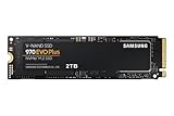
- Always Evolving SSD: The 970 EVO Plus is powered by the latest V-NAND technology and firmware optimization, maximizing the potential of NVMe bandwidth; Comes in storage capacities of up to 2TB, with reliability of up to 1,200 TBW.Computer Platform:PC.Internal Storage : Samsung V-NAND 3-bit MLC. Voltage : 3.3 V 5 % Allowable voltage.Allowable Voltage : 3.3 V 5 % Allowable voltage.
- Breakthrough Read/Write Speeds: The 970 EVO Plus reaches sequential read/write speeds up to 3,500/3,300 MB/s, up to 53% faster than the 970 EVO
- Samsung Magician for Data Security: This software provides a suite of user-friendly tools that help you keep your drive up to date, monitor drive health and speed, and even boost performance
- Superior Heat Dissipation: Samsung’s Dynamic Thermal Guard automatically monitors and maintains optimal operating temperatures to minimize performance drops
- 7 Year Limited Warranty: The 970 EVO Plus provides up to 1200 TBW (Terabytes Written) with 5-years of protection for exceptional endurance powered by the latest V-NAND technology and Samsung's reputation for quality
Why a package-level F-Chip mattered
Higher-capacity packages may combine many NAND dies, which makes routing and signal quality more challenging. The teardown analysis reported an embedded F-Chip in the 48L package. It described the chip as helping create a point-to-point topology between the SSD controller and NAND package, distribute internal I/O buses among NAND dies, reduce stub-related signal reflections and capacitive loading, and provide retiming support for timing margins.
According to that analysis, one F-Chip connected to eight V-NAND dies; two were used in the analyzed 16-die package. Its reported die area was approximately 0.057 mm². This is a package-architecture change, not a consequence of adding 16 cell layers. It addresses the practical problem of moving signals among a larger set of dies; the available analysis does not establish a universal benchmark uplift for SSDs using it. The package findings are detailed in EE Times’ TechInsights comparison.
Best Value

- GROUNDBREAKING READ/WRITE SPEEDS: The 990 EVO Plus features the latest NAND memory, boosting sequential read/write speeds up to 7,150/6,300MB/s*. Ideal for huge file transfers and finishing tasks faster than ever.
- LARGE STORAGE CAPACITY: Harness the full power of your drive with Intelligent TurboWrite2.0's enhanced large-file performance—now available in a 4TB capacity.
- EXCEPTIONAL THERMAL CONTROL: Keep your cool as you work—or play—without worrying about overheating or battery life. The efficiency-boosting nickel-coated controller allows the 990 EVO Plus to utilize less power while achieving similar performance.
- OPTIMIZED PERFORMANCE: Optimized to support the latest technology for SSDs—990 EVO Plus is compatible with PCIe 4.0 x4 and PCIe 5.0 x2. This means you get more bandwidth and higher data processing and performance.
- NEVER MISS AN UPDATE: Your 990 EVO Plus SSD performs like new with the always up-to-date Magician Software. Stay up to speed with the latest firmware updates, extra encryption, and continual monitoring of your drive health–it works like a charm.
What the die-thickness comparison does—and does not—show
The same analysis reported approximately 132 µm for the earlier 16-die stacked configuration and approximately 36 µm for the analyzed 48L-era 16-die stack. A related EE Times first-look article described roughly 40-µm-class 48L dies and a 16-die wire-bonded package. These are measurements tied to the analyzed stacked-die or package configuration, not an intrinsic thickness specification for every die of either generation. Thinning supports high-die-count packaging and package-height management; it should not be read as a direct measure of NAND electrical performance. See EE Times’ 48L first look.
Does more layer count mean a faster or more reliable SSD?
Not on its own. Layer count is primarily a density and manufacturing-scaling measure. A finished SSD’s speed depends on NAND interface behavior, controller design, populated channels, dies and planes accessed in parallel, firmware, cache policy, thermal limits and workload. The F-Chip was intended to improve signaling and timing conditions in a multi-die package, but that does not guarantee that every 48L SSD will outperform every 32L SSD in a benchmark.
Reliability is similarly product-specific. Samsung’s 32L announcement claimed approximately twice the write endurance and 20% lower power than comparable planar MLC-based drives; those were claims about 32L V-NAND products against a planar comparison, not evidence that 48L universally improved on 32L by those amounts. Cell mode, controller, firmware, overprovisioning and workload affect endurance and power. Samsung’s V-NAND white paper discusses the wider product context, while its MLC-versus-TLC white paper addresses SSD-level considerations.
Was 48L immediately cheaper to make?
The purpose of increasing density was to improve the economics of storing bits, but the available comparison does not provide a universal, directly comparable 32L-versus-48L cost-per-bit figure. More masks, higher-aspect-ratio etches and tighter yield control can add complexity during manufacturing ramp-up. Whether that complexity pays off depends on yield, wafer throughput, process maturity, test and package costs, and production scale. Higher capacity per die can create a path to lower cost per bit; it does not prove that every 48L part was cheaper to manufacture immediately.
How to read the comparison without overclaiming
- Die capacity is not drive capacity. A 256-Gb die equals 32 GB in decimal terms, but package and SSD capacities depend on die count, bad blocks, overprovisioning, controller organization and formatting.
- Layer count is not total string height. The 48L label refers to the memory-cell gate stack, not every select gate, dummy structure or contact.
- Product family names do not prove a specific NAND revision. EE Times associated 48L V-NAND with products including SSD T3, 850 EVO V2, PM971-NVMe and PM1633a, but product implementation and revision matter; a model name alone is not a guarantee about every unit.
- Teardown details are not official Samsung specifications. Die areas, aspect ratios, mask counts, peripheral-area changes, metal features and F-Chip dimensions above are attributed to TechInsights analysis reported by EE Times. Samsung’s public releases establish generation and capacity milestones, not a complete design specification.
- Process-node shorthand can mislead. EE Times’ process discussion references a 20-nm bitline half-pitch, while another comparison describes an approximately 21-nm process node. Those measurements are not interchangeable, so “48L is 20-nm NAND” is too imprecise without defining the metric.
The engineering takeaway
The 32L-to-48L transition shows why 3D NAND generations cannot be judged by layer count alone. Samsung increased the vertical cell stack, but also enlarged the array’s share of the die, reduced some peripheral regions, added a metal feature, addressed multi-die signaling with an F-Chip, thinned dies for dense packaging and accepted more demanding process integration. The vertical expansion was the headline; the broader architecture and manufacturing work made the generation change meaningful.
Quick Recap
Product prices and availability are accurate as of the date/time indicated and are subject to change. Any price and availability information displayed on Amazon at the time of purchase will apply.

