Some links on this page are affiliate links: if you buy through them we may earn a commission, at no extra cost to you.
Pragmatic Semiconductor opened Pragmatic Park in Meadowfield, County Durham, on March 27, 2024. The company describes its manufacturing line as the UK’s first 300-mm semiconductor wafer-fabrication line. It does not make conventional high-performance silicon processors: it produces thin, bendable flexible integrated circuits, or FlexICs, for applications such as RFID, sensing, smart packaging and simple control.
That distinction matters. Pragmatic’s facility is a semiconductor manufacturing milestone, but it represents a different direction from the race toward smaller silicon transistor nodes. Its goal is to put inexpensive, low-complexity intelligence onto objects that are too thin, flexible, curved, disposable or cost-sensitive for a conventional packaged chip.
At a glance
| Company | Pragmatic Semiconductor |
|---|---|
| Facility | Pragmatic Park, St John’s Road, Meadowfield, Durham, DH7 8RJ |
| Official opening | March 27, 2024 |
| Technology | IGZO thin-film transistor FlexICs on flexible polyimide substrates |
| Manufacturing format | 300-mm carriers, approximately 12 inches in diameter |
| Applications | RFID and NFC-related products, sensing, smart packaging, wearables, industrial automation and authentication |
| Planned site capacity | Up to nine fabrication lines |
The opening was marked by HRH The Princess Royal. Pragmatic’s announcement called the site the UK’s first 300-mm semiconductor wafer-manufacturing facility, while its current material presents Pragmatic Park as an expanding manufacturing site. The opening itself was in 2024, not 2026; later company announcements concern platform development and expansion.
What’s actually slowing this PC down?
Pick the symptom - the matching free tool is one click away.
Why 300 mm matters—and what it does not mean
A 300-mm wafer is roughly 12 inches across and provides substantially more usable area than smaller wafer formats. If the process, equipment, handling and yield are suitable, a larger format can produce more devices per run and improve manufacturing economics.
#1 Best Overall

- All-in-One Precision Screwdriver Set - This 62-in-1 precision screwdriver set kit is a complete small screwdriver bit set designed for daily electronics maintenance. The electronics bit set includes 58 screwdriver bits (Phillips, Flathead, Hex, Torx, Torx Security, Pentalobe Screwdriver and more), Screwdriver Handle, Flexible Shaft, Extension Rod, and 1/4" Driver Adapter for versatile repair tasks.
- Wide Compatibility - This precision set supports repairs for phones, iPads, MacBooks, PCs, Laptops, Tablets, Cameras, Watches, Glasses, and Game Consoles. Works well as a console repair kit for PS4, PS5, and controllers and other small devices. A reliable solution for both DIY users and technicians working on modern electronics.
- Durable Cr-V Bits - Built with high-quality Cr-V steel, this electronic bit set delivers superior strength and wear resistance for daily repairs. Precision-machined bits provide a snug fit, helping reduce stripping and extend the life of both screws and tools. A true precision driver set for daily electronic repairs.
- Magnetic & Ergonomic Design - This mobile repair kit also works perfectly as a phone repair kit, featuring strong magnetic tips to hold screws securely. The ergonomic, non-slip handle ensures comfortable control, while the flexible shaft allows easy access to tight or recessed spaces.
- Portable & Organized - A portable precision toolkit packed in a compact storage case keeps all tools organized and easy to carry. This repair tool kit is ideal for home use, office repairs, or on-the-go electronics maintenance.
Pragmatic says each fabrication line can produce billions of chips per year, and that Pragmatic Park has capacity to host up to nine lines. Those are capacity and company-output claims, not evidence that nine lines were operating when the site opened. Actual output depends on die size, wafer utilization, yield, test coverage, product mix and line utilization.
Most importantly, 300 mm describes the manufacturing carrier scale, not transistor performance. Pragmatic’s line is not equivalent to a 300-mm advanced silicon logic fab. Its flexible substrate is prepared on a reusable glass carrier and processed using thin-film transistor technology. The wafer diameter says something about production format; it does not imply the computational capability of a modern silicon CPU.
What is a FlexIC?
A FlexIC is an integrated circuit built on a flexible polyimide substrate rather than a conventional rigid silicon die package. Pragmatic’s platform uses indium gallium zinc oxide, or IGZO, thin-film transistor NMOS technology.
Quick wins for a faster PC:
Repair Windows errors before they cause bigger problemsFix Now →Scan for outdated or missing drivers - takes under a minuteDriver Scan →The result is intended to be extremely thin, light and bendable. Pragmatic describes the technology as a way to “connect, sense and compute” inside objects that traditionally could not economically carry a rigid chip. A label, package, curved product surface or high-volume disposable item may benefit more from a very thin custom circuit than from a conventional microcontroller.
According to Pragmatic’s published Gen 3 specifications, the platform includes:
- 600-nm minimum channel dimension for the n-type transistor.
- IGZO TFT NMOS processing.
- Four metal layers.
- 4-µm routing pitch.
- 1-µm line width and spacing.
- A dedicated 200-kΩ-per-square resistor layer.
- Metal-insulator-metal capacitors rated at 4.5 fF/µm².
- Approximately 37 µm thickness including wafer-level packaging.
- A published minimum bend radius of approximately 5 mm.
These are Pragmatic’s platform specifications, not independent test results. The safe bend radius of a finished product can be different after attachment, lamination, encapsulation or integration with an antenna and packaging.
FlexICs versus conventional silicon chips
| Feature | Pragmatic FlexIC | Conventional silicon IC |
|---|---|---|
| Semiconductor technology | IGZO thin-film transistor platform | Silicon CMOS or another silicon process |
| Substrate | Flexible polyimide supported on a glass carrier during processing | Usually a silicon wafer, followed by packaging |
| Physical form | Very thin and bendable | Typically a rigid packaged component |
| Best fit | Identification, sensing, simple control and flexible integration | Applications ranging from basic controllers to CPUs, memory and complex wireless systems |
| Primary design objective | Low-cost, thin, customizable electronics at high volume | Performance, density, functionality and ecosystem breadth |
| Main limitation | Lower complexity and performance envelope | Can be too rigid, costly or integration-heavy for some thin and disposable products |
“Flexible” also does not mean indestructible. Repeated bending, creasing, torsion, moisture, heat, adhesives and mechanical stress can affect the finished product. Product-specific reliability and qualification remain necessary.
Free tools Windows power users keep installed
One-click scans. No signup required.
Rank #2
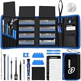
- 【Wide Application】This precision screwdriver set has 120 bits, complete with every driver bit you’ll need to tackle any repair or DIY project. In addition, this repair kit has 22 practical accessories, such as magnetizer, magnetic mat, ESD tweezers, suction cup, spudger, cleaning brush, etc. Whether you're a professional or a amateur, this toolkit has what you need to repair all cell phone, computer, laptops, SSD, iPad, game consoles, tablets, glasses, HVAC, sewing machine, etc
- 【Humanized Design】This electronic screwdriver set has been professionally designed to maximize your repair capabilities. The screwdriver features a particle grip and rubberized, ergonomic handle with swivel top, provides a comfort grip and smoothly spinning. Magnetic bit holder transmits magnetism through the screwdriver bit, helping you handle tiny screws. And flexible extension shaft is useful for removing screw in tight spots
- 【Magnetic Design】This professional tool set has 2 magnetic tools, help to save your energy and time. The 5.7*3.3" magnetic project mat can keep all tiny screws and parts organized, prevent from losing and messing up, make your repair work more efficient. Magnetizer demagnetizer tool helps strengthen the magnetism of the screwdriver tips to grab screws, or weaken it to avoid damage to your sensitive electronics
- 【Organize & Portable】All screwdriver bits are stored in rubber bit holder which marked with type and size for fast recognizing. And the repair tools are held in a tear-resistant and shock-proof oxford bag, offering a whole protection and organized storage, no more worry about losing anything. The tool bag with nylon strap is light and handy, easy to carry out, or placed in the home, office, car, drawer and other places
- 【Quality First】The precision bits are made of 60HRC Chromium-vanadium steel which is resist abrasion, oxidation and corrosion, sturdy and durable, ensure long time use. This computer tool kit is covered by our lifetime warranty. If you have any issues with the quality or usage, please don't hesitate to contact us
How the manufacturing process differs from silicon
Pragmatic prepares polyimide on a glass carrier and builds thin-film transistors and interconnect layers on that flexible substrate. The process uses semiconductor manufacturing techniques, including photolithography, but it is not conventional silicon CMOS.
The company says its process has significantly fewer steps than conventional silicon manufacturing and uses lower temperatures, less energy, less water and fewer harmful gases. A simplified description is:
- A flexible polyimide substrate is prepared on a reusable glass carrier.
- Thin-film transistor layers are formed using the IGZO process.
- Photolithography patterns the device and interconnect structures.
- Metal layers, resistors, capacitors and other platform features are added.
- The wafer-level structure is tested and packaged before the finished FlexICs are separated for product integration.
This should not be read as semiconductor manufacturing without complexity. Customers still need device design, layout, verification, testing, packaging and system integration. Pragmatic says its foundry process can take less than 48 hours, while its current foundry material describes wafer processing as taking only days. That is a fabrication-cycle claim, not a promise that every complete product will be designed, qualified and delivered in 48 hours.
What can the chips do?
RFID, NFC and supply chains
FlexICs can support identification and data interaction in labels, packaging and tracked goods. They may be useful where adding a conventional rigid silicon component to every item is too expensive or physically inconvenient.
The Tool Desk
Outbyte PC Repair FREEClear out junk files and repair common Windows errorsFree Scan →Outbyte Driver Updater FREEFix the driver behind crashes, sound loss and screen glitchesFind Drivers →A working RFID or NFC product still needs more than the chip. Antenna geometry, reader or phone compatibility, operating distance, memory, coupling, product materials, packaging and software all affect the result.
Smart packaging
A package can use a FlexIC for authentication, item-level identification, sensor readout or interaction with a reader. The circuit can provide intelligence, but it does not by itself create a complete connected-packaging system. The antenna, sensor, power strategy, application software and commercial workflow must also be designed.
Sensing and industrial control
Pragmatic lists sensor readout, multiplexing and driver circuitry among its target functions. These can support factory automation, supply-chain monitoring and flexible controllers where the required computation is modest.
Rank #3
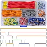
- Complete Specification: 840 pcs jumper wires in 14 precise lengths (3mm, 5mm, 7mm, 10mm, 12mm, 15mm, 17mm, 20mm, 22mm, 25mm, 50mm, 75mm, 100mm, 125mm), 60 pieces for each length. Perfectly meets basic to complex connection needs in breadboard and circuit projects.
- High-Quality Material: Made of premium copper-plated core with excellent conductivity, ensuring stable signal transmission. The outer insulating layer is flexible, durable, and safe to use, preventing short circuits and ensuring long-term reliability.
- Easy to Use: All wires are pre-stripped (no need for manual peeling) and pre-formed with right angles, making them easy to insert into breadboards or circuit boards. Flexible enough to bend and reshape for tight spaces—no soldering required, saving time for DIY enthusiasts.
- Organized Storage: Packed in a sturdy plastic case with separate compartments for each length. Keep wires neat, easy to identify, and prevent loss—ideal for quick access during projects at home or lab.
- Wide Applications: Essential for electronic DIY projects, Arduino experiments, PCB circuit testing, and more. Compatible with computers, electronic communications, instruments, industrial controls, digital cameras, LCM/LCD displays, and other electronic devices.
Wearables and curved products
The thin form factor can help products that must conform to curved surfaces or remain comfortable and unobtrusive. Whether it is suitable depends on the final assembly’s bend cycle, environmental exposure and mechanical design—not simply the platform’s nominal 5-mm bend-radius figure.
Security and authentication
Flexible circuits can be embedded in labels, products or packaging for authentication and anti-counterfeit workflows. The strength of the system depends on the security architecture, backend software, reader infrastructure and resistance to copying or removal.
Capacity, investment and regional impact
The 2024 opening announcement said Pragmatic Park could host up to nine fabrication lines, with each line capable of producing billions of chips per year. Pragmatic also announced an expectation of at least eight UK manufacturing lines over the following five years and projected more than 500 highly skilled jobs across the North East and Cambridge.
In December 2023, the company announced a Series D investment with a £162 million first close and a planned second close that brought the announced total to £182 million. Investors named by Pragmatic included M&G Catalyst, the National Wealth Fund—then called UK Infrastructure Bank—Northern Gritstone, Latitude, MVolution Partners, British Patient Capital, Cambridge Innovation Capital and Prosperity7 Ventures.
The funding was intended to accelerate UK manufacturing expansion. It should not be interpreted as money spent entirely on the single line opened in March 2024.
Do these 3 things before closing this tab:
1Fix the driver behind crashes, sound loss and screen glitches2Repair Windows errors before they cause bigger problems3Scan for outdated or missing drivers - takes under a minutePragmatic also lists production activity at NETPark in Sedgefield, County Durham, alongside its Meadowfield site. The Durham footprint and Cambridge operations are part of a broader regional manufacturing and engineering strategy, but the available company material does not establish a complete independently verified count of currently operating lines or current output.
Why the facility matters to the UK semiconductor sector
The facility matters for four separate reasons:
- Domestic manufacturing: It adds UK-based high-volume semiconductor capacity in a category that would otherwise depend on overseas production.
- A differentiated niche: Pragmatic is targeting flexible, low-cost thin-film ICs rather than competing directly with leading-edge silicon logic manufacturers.
- Regional development: The project brings manufacturing, engineering and potentially skilled employment to County Durham and the wider North East.
- Supply-chain resilience: Localized production can shorten some supply chains and give customers another route to custom electronics.
It would be wrong to call this UK semiconductor self-sufficiency. FlexICs do not replace silicon processors, memory, power semiconductors, high-performance sensors or other chip categories. The achievement is specialized capacity, not a complete domestic chip ecosystem.
Rank #4

- 【200 in 1 Screwdriver Kit】This electronic screwdriver tool kit includes 2 non-slip screwdriver handles, precision anti-static tweezers, flexible shaft telescopic rod, 164 screwdriver heads, solid shaft telescopic rod, rubber suction cup, black cleaning brush, 14 triangles Paddle, 2 blue double-ended plastic opening tool and 2 pointed opening tool, metal opening tool, magnet, magnetic pad and Oxford cloth bag.
- 【Best Combination】This electronic repair kit has 164 different bits, a sturdy flexible shaft, opening tool, ESD tweezers, etc. It is not just a complete repair kit for mobile phones, watches, glasses, cameras, tablets, laptops,PC, TVs and other electronic devices. The 1/4 inch bit can be applied to various scenes in life. After a complete redesign, it can provide all the tools you need, but not the tools you don't need.
- 【High Quality Material】All bits are made of high quality CR-V steel by vulcanization, it's hardness can reach over HRC62°, which is harder than the ordinary steel material and more durable, all of standard size bit undergo the rigorous quality control testing, the tip is stable and not easily stripped.
- 【Humanized Design】Ergonomic and press & push design handle, it is comfortable to hold even for the long-time use. For the bits that are often used in repairing electronic products, have 2pcs or 3pcs or 4pcs in this set, allows you to avoid damage due to repeated use need to buy a new replacement, save your money. And this precision set comes with a storage bag which is made from oxford, offering a whole protection, easier storage and carrying.
- 【Extension and Flexible Shaft】There is an adjustable extension rod and a flexible shaft for some electronics where the screws are not on the surface.You no longer need to laboriously open the screws inside the machine.
The sustainability case—and its limits
Pragmatic says its thin-film process uses fewer process steps, less energy and water, and fewer harmful gases than standard silicon manufacturing. Its ESG report says Pragmatic Park has operated on 100% renewable electricity since its official opening in April 2024, reports more than 95% less electricity per wafer than a typical silicon fab, and reports water consumption of approximately 40 litres per wafer.
These figures are company-reported comparisons. “A typical silicon fab” does not identify a particular process, product, facility or functional equivalent. A per-wafer comparison also does not automatically show lower impact per working chip or per complete product.
A full life-cycle assessment would need to consider polyimide, glass carriers, metals, packaging, antennas, assembly, transport, end-of-life handling and the reader or device ecosystem. Renewable electricity can reduce operational electricity emissions, but it does not by itself establish a complete product carbon footprint.
Independent reader supportYour contribution helps us test, update, and keep practical guides available for everyone.How customers access the technology
Pragmatic offers a FlexIC foundry model for customers that want custom flexible circuits. Its Gen 3 platform includes technology files, device models, primitive libraries, parameterized cells, design-rule and layout-versus-schematic checks, and tape-out guidance. Pragmatic says the platform supports Cadence and Siemens EDA tools.
A typical path is:
- Discuss the application, required functions, volumes and integration requirements with Pragmatic.
- Request access to the platform and PDK through the FlexIC Foundry.
- Design and verify the circuit using the supported tools and process rules.
- Tape out the design for fabrication.
- Integrate the fabricated FlexIC with its antenna, sensor, package or other product hardware.
- Test and qualify the complete product for its intended environment.
Pragmatic says tape-out to delivery can take a few weeks, but this is not a universal guarantee and does not include every stage of product engineering or regulatory qualification. PDK access and manufacturing terms are not publicly listed as a universal price schedule.
For academic and research users, Pragmatic identifies EUROPRACTICE as its official partner for multi-project wafer runs. Pricing and availability depend on the specific run, institution and design.
Recommended Free Tools
Fab-as-a-Service and “Fab-in-a-Box”
Pragmatic uses “Fab-as-a-Service” to describe a modular approach to localized FlexIC manufacturing. It has also described a “Fab-in-a-Box” concept that could support co-located, end-to-end production at customer sites.
Best Value
- Solder-Free Prototyping: The 830-point breadboard allows you to plug in components and wires directly — no soldering required. Build, test, and modify circuits quickly and easily.
- Organized & Portable: All items come packed in a durable storage box, making it easy to keep your workspace tidy and take your projects on the go.
- Rich Wire Selection: With 140 rigid breadboard wires, 65 flexible jumpers, and 120 Dupont pins in all three gender types (M/M, M/F, F/F), you'll always have the right connector for any connection.
- Wide Compatibility: Perfectly suited for Arduino UNO R3, Mega 2560, Nano, Raspberry Pi 4/3/2/Zero, ESP32, ESP8266, STM32, and various sensors, relays, displays, and modules.
- Perfect for Learning & Teaching: An excellent choice for STEM education, school science projects, electronics workshops, and hobbyist experimentation.
This is a manufacturing and business model, not a cloud subscription or an instant general-purpose chip factory. A serious deployment would need answers about the included equipment, ownership and operation, cleanroom requirements, chemicals, gases, water, power, safety systems, supported process generations, minimum volumes, engineering support, intellectual property and qualification.
The company’s public material explains the concept but does not answer all of those commercial and engineering questions. Customers should treat it as a model to evaluate with Pragmatic rather than as an off-the-shelf fab available without site preparation or specialist staff.
When FlexICs are a strong fit
- The product needs an extremely thin, light or bendable chip.
- The function is identification, sensing, simple control, multiplexing or data interaction.
- Unit cost and low non-recurring engineering cost matter more than processing performance.
- The product is manufactured in high volumes or attached to packaging and labels.
- Rapid design iteration is valuable.
- A custom ASIC-like function is needed without commissioning a conventional silicon process.
When conventional alternatives may be better
A FlexIC may be a poor fit when the application needs a high-performance processor, large memory, advanced wireless baseband, high current, high speed, demanding analog precision or a mature software ecosystem. Conventional silicon may also be preferable for high-temperature, harsh-environment or safety-critical products unless the complete FlexIC-based design has been specifically qualified.
Other options include conventional silicon RFID or NFC ICs, silicon microcontrollers, printed electronics, flexible PCBs, rigid-flex assemblies and other thin-film platforms. A flexible PCB may be the better answer when conventional packaged components can remain rigid and only the interconnect needs to bend. Printed electronics may suit simple conductive traces, sensors or displays but not necessarily a mixed-signal ASIC.
What has changed since the opening?
Since the 2024 ceremony, Pragmatic has promoted its Gen 3 platform for mixed-signal flexible ASIC design, introduced newer offerings including NFC Connect, and described construction or development of additional manufacturing capacity. Its company material also states an ambition to become the UK’s largest semiconductor manufacturer by wafer volume.
Those later statements describe company plans, positioning and expansion claims. They should not be confused with independently verified current output or proof that the full planned capacity is already operational.
The bottom line
Pragmatic’s Durham facility is significant because it expands the definition of what a semiconductor fab can target. It is not a smaller version of an advanced silicon CPU plant. It is a specialized 300-mm manufacturing line for thin-film, flexible circuits designed to add simple intelligence to billions of objects.
PC Slower Than It Used to Be?
A free scan shows the junk files, broken settings and background clutter dragging Windows down - then fixes them in one click.Free scan · Windows 10 & 11Outdated Drivers Are Slowing You Down
One free scan finds every outdated or missing driver and matches the right update for your exact hardware.Free scan · exact hardware matchFor RFID, sensing, smart packaging, wearables and industrial identification, that combination of thinness, bendability, customization and potential volume can be valuable. For processors, large memories and demanding silicon workloads, it is the wrong comparison. The UK milestone is real—but its importance lies in a differentiated manufacturing model, not in matching conventional silicon on transistor density or computing performance.
Read Pragmatic’s opening announcement and its Gen 3 platform specifications.
Quick Recap
Product prices and availability are accurate as of the date/time indicated and are subject to change. Any price and availability information displayed on Amazon at the time of purchase will apply.

