What’s actually slowing this PC down?
Pick the symptom - the matching free tool is one click away.
A junction field-effect transistor (JFET) is a three-terminal, majority-carrier transistor whose reverse-biased p–n junction gate controls the width of a conducting channel between source and drain. Conventional JFETs are depletion-mode devices: an n-channel part conducts at VGS = 0 and is driven toward cutoff by making the gate negative relative to the source; a p-channel part uses opposite polarities. The gate has very low DC current, but leakage, capacitance and breakdown limits are real design concerns.
What a JFET is
The source and drain carry the channel current; the gate is a p–n junction formed alongside the channel. Reverse-biasing that junction expands its depletion region, narrowing the channel and increasing its resistance. JFETs are voltage-controlled devices and use majority carriers: electrons in n-channel devices and holes in p-channel devices.
The gate is not insulated by an oxide as in a MOSFET. Its normal current is therefore small rather than literally zero, and excessive forward or reverse gate voltage can damage the junction.
Physical structure and polarity
N-channel
An n-type channel joins source and drain. Heavily doped p-type gate regions form reverse-biased junctions with it. At zero gate bias the channel is relatively open; a negative VGS widens the depletion region and reduces current. The symbol arrow identifies the junction polarity, but the channel label is the safer way to identify the device.
#1 Best Overall

- ALLECIN 2N5457 is a bipolar junction triode- Perfectly suitable for variety electronic experiments.
- Gate Current: 10mA; Drain−Gate Voltage: 25V.
- Features: N−Channel for higher gain & Drain and source interchangeable & High ac input impedance & High dc input Resistance & Low transfer and input capacitance & Plastic encapsulated package.
- Widely Application: diy project & low level audio amplifier & switching transistors & analog switching.
- Humanized packaging for easy storage and use. ### Please confirm the data before purchasing.
P-channel
A p-type channel and n-type gate regions provide complementary operation. Positive gate-to-source voltage increases reverse bias, and holes carry current. Voltage and current reference directions must be defined explicitly rather than inferred from a simple “reversed” diagram.
How current is controlled
Zero gate bias
With an n-channel JFET at VGS = 0, applying VDS initially produces a channel-resistance current. As VDS rises, the channel narrows near the drain.
Increasing reverse bias
Making VGS more negative increases depletion width, raises channel resistance and lowers ID. At the device-specific VGS(off), current approaches zero. P-channel polarities are opposite.
Rank #2

- 434 pcs 24 values Transistor Assortment Box
- Includes BJT, Mosfets, JFET, Darlington, Germanium, NPN and PNP Transistors:
- BJTs: 2n3904, 2n3906, 2n5551, 2n5401, C945, A733, C1815, A1015, SS8050, SS8550, S9014, S9015, BC327, BC337, BC547, BC557, BC548, BC558, 2n5088, 2n2222
- MosFET: 2n7000, Darlington: BC517, Germanium: 3AX31, JFET: J201
- Transistors come sorted accordingly in a labeled and handy box, includes 20 pcs Transistor Sockets
Operating regions
| Region | Behavior | Important qualification |
|---|---|---|
| Ohmic (linear or triode) | Acts approximately as a voltage-controlled resistor. | Useful for attenuators and analog switching; resistance depends on voltage and signal level. |
| Pinch-off (saturation) | Drain current changes only weakly with further VDS increase. | It is not zero current and is not destructive breakdown. |
| Cutoff | ID is approximately leakage current when VGS ≤ VGS(off) for the usual n-channel convention. | Cutoff voltage varies between devices and with temperature. |
| Breakdown | Avalanche or junction breakdown causes a sharp current increase. | Exceeding absolute maximum ratings can permanently damage the part. |
In one signed n-channel convention, saturation begins near VDS ≈ VGS − VGS(off). The ohmic-region idealized equation is ID = (2IDSS/VP2)[(VGS−VP)VDS−VDS2/2], when VP is defined as a positive pinch-off magnitude.
Free tools Windows power users keep installed
One-click scans. No signup required.
Shockley transfer equation
In the constant-current region, the first-order n-channel model is:
ID = IDSS[1 − VGS/VGS(off)]2.
- IDSS: drain current at VGS = 0 under specified VDS.
- VGS(off): gate voltage that reduces current to a specified near-zero value.
- The p-channel form uses corresponding reversed polarities.
For IDSS = 10 mA, VGS(off) = −4 V and VGS = −1 V, the estimate is 10(1−0.25)2 = 5.625 mA. This is an illustrative model, not a guaranteed production current.
Rank #3
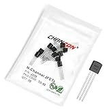
- Transistor Type: Junction Field-Effect Transistor (JFET) with N-Channel Polarity.
- N-Channel JFET: Specialized for high impedance and frequency applications, including signal amplification and switching.
- Specification: Capable of managing Drain-Source voltage (VDSS) up to 25V and Drain Current (ID) up to 0.06A.
- Application: Ideal for use in electronic circuits such as signal amplifiers and high frequency applications.
- Package: Packed in an Anti-Static bag for electrostatic protection, ensuring ESD safety and long shelf life.
Datasheets often give broad minimum and maximum ranges for both parameters. Use those limits, temperature data and the actual operating region rather than designing from typical values alone.
Pinch-off versus cutoff
| Term | Meaning |
|---|---|
| Pinch-off voltage | May mean the VDS where saturation starts, or a characteristic gate-voltage magnitude, depending on the textbook. |
| VGS(off) | Gate-to-source voltage producing near-zero drain current under a specified test definition. |
Some texts write VP as a positive magnitude; others use a signed voltage. Define the convention before substituting values. Portland State’s treatment separates the region equations and signed cutoff conditions: textbook material.
Small-signal model
Transconductance is the local current response to gate voltage:
Rank #4

- 2N5458 N-Channel JFET Audio Amplifier 10mA TO-92 Transistor
- Compact Design, Endless Possibilities,Sleek, space-saving TO-92 package – perfect for miniaturized projects like wearables, portable gadgets, or tight PCB layouts without limiting performance.
- Versatile Performance for Every Project,Reliably handles common electronics tasks – from signal amplification to LED driving and low-power switching – making it a go-to for DIY builds and commercial devices alike.
- Built to Last, Even in Tough Conditions,Engineered for durability: withstands temperature fluctuations, resists static shocks, and maintains stability through daily use or harsh environments.
- Effortless Integration,Standard E-B-C pinout works seamlessly with hand-soldering, automated assembly, and most PCBs – simplifies prototyping and mass production for makers and manufacturers.
gm = 2IDSS/|VGS(off)| · [1 − VGS/VGS(off)] = gm0[1 − VGS/VGS(off)].
Real saturation curves have finite output resistance: rd = (∂ID/∂VDS)−1 at fixed gate voltage. For a common-source stage, a useful midband estimate is Av ≈ −gm(RD ∥ rd ∥ RL). A source resistor lowers gain but adds feedback, improves linearity and reduces sensitivity to device spread. Junction capacitances limit high-frequency response; the Delft model discusses output conductance and frequency behavior: Delft JFET reference.
Biasing methods
Fixed-gate bias
An n-channel device receives a negative gate supply. Analysis is simple, but a second supply may be required and parameter variation is poorly compensated.
Best Value

- High Input Impedance
- Low IGSS
- The photo is the actual product image
- The product is strictly screened, the model number remains the same, and the part number changes randomly.
- NOTE:Exposure to absolute maximum rating conditions for extended periods may affect device reliability.
Self-bias
Ground the gate through a large resistor and place RS in the source lead. With VG ≈ 0, VGS ≈ −IDRS. Substitute this relation into the Shockley equation and check both minimum and maximum device parameters.
Voltage-divider bias
A divider establishes a controlled gate voltage, usually with a source resistor. It costs more components but offers a wider bias range.
Independent reader supportYour contribution helps us test, update, and keep practical guides available for everyone.Reading a JFET datasheet
| Parameter | Meaning and design use |
|---|---|
| IDSS | Zero-gate drain current under stated conditions; sets the transfer scale. |
| VGS(off) | Cutoff-voltage range and required control swing. |
| gm or gfs | Current change per gate-voltage change. |
| VBR(GSS) | Gate-source breakdown limit. |
| VDS/VDSS, ID, PD | Voltage, current and thermal limits; power is approximately VDSID and must be derated. |
| Ciss, Crss | Input and reverse-transfer capacitance affecting loading and Miller feedback. |
| Noise, package and pinout | Determine suitability for the source impedance, frequency and physical layout. |
Onsemi’s 2N5457/2N5458 data sheet specifies n-channel depletion devices, a 25 V drain-source rating, −25 V reverse gate-source rating, TO-92 packaging and 310 mW dissipation at 25 °C subject to derating; it also identifies source and drain as interchangeable for that family: onsemi data sheet. InterFET lists through-hole, SOT-23 and die options for its 2N5457 and reports typical room-temperature gate leakage below 10 pA for the cited product, not for every device carrying that number: InterFET data sheet.
Applications and selection
- Common-source amplifiers, source followers and high-impedance sensor inputs.
- Audio and RF front ends where the specified noise matches the source impedance.
- Voltage-controlled resistors, attenuators and automatic-gain-control elements in the ohmic region.
- Simple current limiters, current sources and normally-on startup paths.
- Specialized integrated and high-temperature analog processes.
Select channel polarity, full IDSS and VGS(off) ranges, transconductance, leakage, noise at the intended frequency, gate and drain breakdown ratings, capacitance, temperature range, package, pinout, matching and lifecycle status. Familiar part numbers may come from different vendors, bins or production lots.
Recommended Free Tools
JFETs compared with alternatives
| Characteristic | JFET | BJT | MOSFET |
|---|---|---|---|
| Control | Gate voltage and depletion width | Base-emitter voltage plus base current | Insulated-gate electric field |
| Input current | Low reverse leakage, not zero | Requires base current | Very low steady-state gate current, with oxide limits |
| Typical strength | High-impedance analog and controlled resistance | High transconductance per current in many designs | Broad high-current and switching selection |
| Key limitation | Wide parameter spread and junction-voltage limits | Input current and loading | Gate-oxide ESD and overvoltage vulnerability |
Do not assume JFETs are universally quieter or more linear. Compare voltage and current noise, source impedance, frequency, bias and topology. Depletion MOSFETs provide normally-on behavior without a p–n gate junction, but their oxide-related failure mechanisms differ.
Quick Recap
Common mistakes and failure modes
- Forward-biasing the gate, which raises current and can damage the junction.
- Exceeding gate, drain or power ratings; the onsemi −25 V gate figure is specific to its 2N5457/2N5458 family.
- Calling pinch-off “off”; saturation normally still carries substantial current.
- Applying the Shockley equation in the ohmic region or outside its bias assumptions.
- Using typical parameters without checking production spread, temperature and signal swing.
- Treating a JFET as an ideal switch or assuming every 2N5457 has identical characteristics.
- Ignoring package pinout and electrostatic transients on the gate node.
Product prices and availability are accurate as of the date/time indicated and are subject to change. Any price and availability information displayed on Amazon at the time of purchase will apply.

