Crashes, No Sound, or Screen Glitches?
Random freezes, missing sound and display glitches usually trace back to one bad driver. Find and replace yours safely.Free scan · under a minutePC Slower Than It Used to Be?
A free scan shows the junk files, broken settings and background clutter dragging Windows down - then fixes them in one click.Free scan · Windows 10 & 11Some links on this page are affiliate links: if you buy through them we may earn a commission, at no extra cost to you.
Canada’s chip sector can regain momentum, but not by trying to recreate a leading-edge chipmaking powerhouse. Its more credible path is to build on strengths in photonics, compound semiconductors, sensors, MEMS, specialized imaging, advanced packaging and low-power edge computing—and connect research to repeatable production and paying customers.
A comeback, but not a return to the whole chip stack
“Getting its groove back” is best understood as rebuilding a connected route from research and design to prototypes, specialized manufacturing and commercial products. It does not mean Canada is on the verge of producing every kind of chip at home, or of matching the scale of Taiwan, South Korea or the United States in leading-edge logic.



Canada has retained pockets of semiconductor expertise, but strong university research and design talent do not automatically produce a durable chip industry. Companies also need patient capital, skilled process and packaging workers, access to fabrication, customers willing to qualify new components, and enough production volume to justify investment. Canada’s challenge has been less about having no expertise than about making those pieces work together at commercial scale.
The distinction matters because the semiconductor supply chain is not one activity. Design defines a chip’s function; front-end fabrication builds its structures on a wafer; assembly and testing turn fabricated dies into validated products; and packaging connects and protects them. A country can be good at design or research while relying on overseas factories for wafers and other partners for packaging.
#1 Best Overall
The federal government counted more than 500 Canadian companies involved in semiconductor R&D, design or manufacturing in July 2024, including more than 100 design firms, 30 applied research laboratories and five commercial facilities. That is evidence of breadth, not 500 chip manufacturers or a domestic high-volume foundry base. The government’s announcement also described the sector as a mix of research, design and manufacturing activity.
Why specialization is the more credible bet
A leading-edge logic fab is an exceptionally expensive, long-horizon bet. It needs sustained high utilization, reliable access to equipment and materials, experienced workers, anchor customers and a dense network of suppliers. Canada would be competing against established clusters with far greater scale. That makes a new, conventional megafab a less convincing national strategy than targeted investment in technologies where Canadian research and existing facilities can matter.
That is an assessment of the economics, not a forecast that Canada can never build more wafer capacity. It is also not an argument against manufacturing. It is an argument for choosing the manufacturing and product categories where a smaller ecosystem can plausibly win. Specialized components can serve markets that value particular optical, sensing, power, radio-frequency or packaging capabilities rather than the lowest-cost commodity logic.
Canada’s most plausible opportunities include:
- Compound semiconductors and photonics: materials and devices useful in optical, high-frequency and other specialized applications, including communications and sensing.
- MEMS, image sensors and other sensors: components for industrial inspection, space imaging, medical devices, vehicles, robotics, environmental monitoring and aerospace.
- Advanced packaging: assembling multiple dies or heterogeneous components into systems where interconnects, size and thermal performance matter.
- Low-power edge computing: hardware that processes information near a sensor or device instead of sending every task to a cloud data centre.
- Design and applied research: turning Canadian research into prototypes and products, even when some fabrication steps take place with external foundries.
Invest in Canada identifies compound-semiconductor fabrication and advanced packaging among the country’s strengths, while describing the broader ecosystem as primarily design-focused with manufacturing concentrated in specialized areas. It calls the Canadian Photonics Fabrication Centre in Ottawa North America’s only public compound-semiconductor foundry; that characterization is the agency’s, rather than a claim that Canada has a general-purpose silicon foundry. Its industry overview also lists clusters in Vancouver, Edmonton, Waterloo, Toronto, Ottawa, Montréal and Québec City. Those centres are not interchangeable: their capabilities depend on the companies, labs and facilities located in each.
Compound semiconductors are not substitutes for every silicon processor. Their value is that certain material systems can suit optical, radio-frequency, high-power or high-frequency applications. That makes them relevant to photonics, communications, sensing, defence, space, quantum research and energy systems. Canada can gain strategic value in such segments without claiming leadership across the full semiconductor market.
Packaging offers another avenue, but it should not be confused with wafer fabrication. Front-end processing creates devices on a wafer; back-end assembly and testing package, connect and validate them. Advanced packaging goes further, integrating multiple dies or types of components—sometimes using chiplet or 2.5D/3D approaches—to improve system performance or fit. A stronger packaging capability can complement foreign wafer production; it does not replace it.
FABrIC: building a bridge from design to commercialization
FABrIC is an infrastructure and commercialization network led by CMC Microsystems, not a single chip company. Its intended role is to help businesses access semiconductor design and fabrication resources, develop talent, connect researchers with manufacturing capabilities and move semiconductor-based products toward market.
Do these 3 things before closing this tab:
1Fix the driver behind crashes, sound loss and screen glitches2Clear out junk files and repair common Windows errors3Scan for outdated or missing drivers - takes under a minuteIn July 2024, the federal government announced a $120 million contribution to a project valued at more than $220 million. The announcement projected nearly 325 highly skilled jobs created and about 440 maintained during the five-year project. It also positioned the investment as part of a Canada–U.S. effort to strengthen a cross-border semiconductor manufacturing corridor. Those job figures were projections, not a report of jobs already realized. The announcement sets out the program’s scope and expected effects.
A later round shows what the network is trying to support. In May 2026, FABrIC announced more than $10.7 million for 11 projects, with an estimated total project value of $44.3 million. The projects were selected from 64 expressions of interest; six were in Quebec, four in Ontario and one in British Columbia. The portfolio spans edge AI, photonics, sensors, wearables, ocean monitoring, automotive systems and industrial uses. CMC Microsystems describes the funded projects and their intended commercialization paths.
These projects make the edge-AI strategy more concrete. “AI hardware” does not necessarily mean a Canadian-made rival to a high-end data-centre accelerator. It may mean a low-power controller, sensor, analog inference circuit, radar system or optical connection designed to handle a narrow task close to where data is collected. That can matter in industrial, medical, automotive or remote-monitoring settings, where power, latency, bandwidth or connectivity constrain cloud-based processing.
Rank #3

- Wide Input Voltage Range: Supports 340-550VAC or 480-780VDC input, enabling stable operation in diverse industrial environments with flexible power source compatibility.
- High Efficiency Performance: Achieves up to 92% efficiency with passive PFC, reducing energy loss and heat generation for reliable long-term operation in automation applications.
- Comprehensive Protection Features: Integrated short-circuit, overload, over-voltage, and over-temperature safeguards ensure device safety and durability under demanding conditions.
- Compact Rail Mount Design: Slim 63mm width with TS-35/7.5 or 15 rail mounting, optimizing space utilization in control cabinets while facilitating easy installation and maintenance.
- Industrial Compliance & Certification: Meets UL61010, BS EN/EN61000-3-2, and EMC standards, guaranteeing suitability for industrial controls, manufacturing equipment, and electromechanical systems.
Still, a selected project and a stated path to commercialization are not the same as product revenue, sustained production or market adoption. FABrIC’s success should ultimately be judged by what companies sell and manufacture, not just by the number of applications or funded prototypes.
Teledyne in Bromont: a practical manufacturing example
A $42 million Teledyne project in Bromont, Quebec, illustrates the kind of industrial upgrade that fits Canada’s specialized path. The federal government announced an $8 million contribution toward moving a specialized CCD image-sensor production line from 150 mm to 200 mm wafers. The announcement projected 40 new jobs and more than 560 jobs maintained. It said the larger wafers could yield 1.8 times as many chips and improve productivity and efficiency by 40%; those figures are claims in the government announcement, not independently audited results presented here. The release provides the project details.
This is not a leading-edge smartphone or AI-processor fab. It is a targeted modernization of a specialized imaging capability with an existing industrial base. That distinction is precisely why the example matters: public funding can upgrade equipment and extend a production line without attempting to finance an entirely new megafab. Teledyne operates wafer fabs in Bromont and Edmonton, and the government says the Canadian facilities are available to Canadian small and medium-sized enterprises and research centres for prototyping or volume production.
Whether an upgrade becomes a durable advantage depends on more than wafer diameter. It also depends on utilization, customer demand, yields, qualification requirements and the company’s ability to keep investing. But an existing facility serving specialized imaging markets is a more grounded starting point than a broad promise of domestic self-sufficiency.
IBM and C2MI: packaging capacity, not a finished result
In November 2025, the federal government announced up to $210 million toward a $662 million IBM Canada/C2MI project to expand advanced packaging and commercialization capabilities at IBM’s Bromont facility and C2MI. The government said the project was intended to add next-generation packaging and R&D capacity, create 75 highly skilled jobs and maintain more than 1,000 jobs in the Bromont region. These are terms and projections from the announcement; “up to” funding is not proof that the full amount has been disbursed, and announced capacity is not the same as operational production. The government’s release describes the project.
What’s actually slowing this PC down?
Pick the symptom - the matching free tool is one click away.
Rank #4
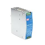
- Original and Genuine NDR-120W|(12V 10A).(24V 5A).(48V 2.5A) For Industrial automation control system,Semiconductor fabrication equipment,Electro-mechanical apparatus
- The NDR-120 series relevant certificates for industrial control apparatus (UL508, TUV BS EN/EN62368-1, and etc.) is a very competitive power supply solution for industrial applications.
- Input 90-264Vac, in line with German industrial standard thin economical power supply
- The metal shell has good heat dissipation, stable operation in the environment of -20? to 70?, and the efficiency is as high as 89%
- It is equipped with constant current mode for over-load protection, fitting various inductive or capacitive applications.
The strategic logic is sound: as systems increasingly combine different kinds of chips, packaging and integration can be important sources of performance and product differentiation. The practical test is what equipment is installed, which capabilities are available to customers, how the facility is used and whether commercial products emerge. Packaging is a valuable part of the chip supply chain, but it does not mean Canada has become self-sufficient in front-end wafer fabrication.
Independent reader supportYour contribution helps us test, update, and keep practical guides available for everyone.The bottleneck is converting capability into repeat business
Research infrastructure and public grants can help a company reach a prototype. They cannot by themselves guarantee a market. A semiconductor startup may need years of development before customers will qualify a component, especially in automotive, medical, aerospace and defence applications. It must find capital for that interval, secure access to electronic-design-automation tools and fabrication, protect or license intellectual property, and build the process expertise required for reliable production.
Canada also needs people beyond chip designers: process engineers, packaging specialists, cleanroom technicians, equipment-maintenance staff and executives who have taken semiconductor products through manufacturing and sales. A healthy ecosystem must retain graduates and experienced workers, while giving Canadian industrial firms reasons to buy locally developed components. If Canadian companies design chips that are fabricated abroad and the products are then sold mainly to foreign customers, the work may still be valuable—but it will not create a self-contained domestic supply chain.
There are real trade-offs. Specialized products can be defensible, but their markets may be smaller than those for commodity processors. Public support can make shared infrastructure and long-cycle research possible, but funding can also keep projects moving without proving customer demand. Cross-border integration with the United States offers access to scale, customers and a broader supply chain, yet it can leave higher-value production or ownership elsewhere. And local production may cost more than importing a component, even when it provides resilience or strategic value.
The Tool Desk
Outbyte Driver Updater FREEFix the driver behind crashes, sound loss and screen glitchesFind Drivers →Outbyte PC Repair FREERepair Windows errors before they cause bigger problemsFix Now →That resilience can be significant. Chips underpin communications, vehicles, medical technology, aerospace, defence, energy systems and AI. Supply disruptions and export controls have raised the value of dependable capacity in Canada and allied countries. But “strategic capability” is not the same as semiconductor independence: Canadian firms will continue to rely on international suppliers, equipment, materials, foundries and markets.
How to tell whether the strategy is working by 2030
The most useful scorecard looks beyond announcements and company counts. Over the next several years, evidence of a genuine recovery would include:
- Products and customers: Canadian-designed chips or semiconductor-based systems reaching production and earning revenue from repeat customers.
- Continuous manufacturing: facilities running sustained production, with demonstrable utilization and access for companies beyond one-off research projects.
- Private follow-on investment: public contributions drawing additional private capital and helping firms finance the long path from prototype to qualified product.
- Exports and commercial reach: specialized components finding markets outside government-supported programs and beyond a single domestic buyer.
- Talent retention: skilled graduates and experienced workers moving into Canadian industry and staying through scale-up.
- Supply-chain depth: dependable access to packaging, testing, design services and fabrication at home or through resilient allied partnerships.
- Repeatability: multiple companies using the ecosystem successfully, rather than a handful of isolated grants or facilities carrying the whole story.
One small-volume sensor for a space or medical application may have greater strategic value than a much larger volume of easily substituted parts. The test is not whether every Canadian project becomes a mass-market success; it is whether the ecosystem can repeatedly turn specialized expertise into products customers need.
Canada’s realistic chip-sector ambition
Canada has credible ingredients for a more consequential semiconductor sector: research and design talent, specialized manufacturing, photonics and sensor capabilities, packaging infrastructure and new programs intended to connect them. The emerging strategy is narrower than building a complete domestic chip industry—and more plausible for that reason.
Free tools Windows power users keep installed
One-click scans. No signup required.
The comeback will be real if those capabilities produce durable businesses, sustained production, exports and skilled jobs. Until those results are visible, funding announcements and promising project portfolios are signs of investment, not proof of recovery. Canada can become a valuable node in North American and global supply chains without making every chip at home; its challenge is to ensure it captures enduring industrial value from the parts of the supply chain it is best placed to serve.
Quick Recap
Product prices and availability are accurate as of the date/time indicated and are subject to change. Any price and availability information displayed on Amazon at the time of purchase will apply.

