Some links on this page are affiliate links: if you buy through them we may earn a commission, at no extra cost to you.
GUC announced on January 10, 2024, that it had taped out a UCIe physical-layer (PHY) IP design supporting 32 Gbps per lane on TSMC’s N3P process and in a CoWoS package. The milestone concerned an interconnect building block for chiplets—not a finished processor or a claim of mass production. GUC later announced the launch of 32G UCIe silicon in March 2025, describing it as supporting UCIe 2.0.
What GUC taped out
The design was a UCIe PHY IP block: circuitry that sends and receives high-speed signals between dies inside a package. GUC said it used TSMC’s N3P 3nm process and CoWoS advanced packaging, and targeted AI accelerators, high-performance computing (HPC), xPUs and networking devices. GUC called it the first UCIe IP supporting 32 Gbps; that “first” is the company’s claim. GUC’s January 2024 announcement also reports bandwidth density of 10 Tbps per millimeter of die edge, or 5 Tbps/mm full-duplex.
These figures describe an IP design and its stated interface capability. They do not mean GUC had introduced a complete chiplet processor, or that a customer product was already shipping.
UCIe: a connection between chiplets
UCIe, or Universal Chiplet Interconnect Express, is an open standard for communication between dies integrated into the same package. It specifies a physical layer, die-to-die adapter and protocol-related elements, along with a software model and compliance framework intended to help chiplets from different suppliers interoperate. It is not an ordinary board-level connection between separate cards. The UCIe Consortium’s specifications describe the standard and its capabilities.
#1 Best Overall
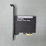
- 【PCILeech Friendly】64-bit Memory Access, PCIe TLP access, and PCILeech compatible. PCILeech utilizes the PCIe board with FPGA DMA to read and write to the target system memory. Note: our card does not come with any custom firmware.
- 【On/Off Switch】You can deactivate your card using the built-in on and off switch, eliminating the need to physically disconnect the device from your PC when you are not using the device.
- 【Layered Cooling】DMA card comes with an included heat sink ensuring optimal performance and longevity! This heatsink is further enhanced by a durable aluminum alloy cover. This layered cooling design helps prevent FPGA thermal throttling and overheating.
A chiplet design can split a large system into dies with different roles—such as compute, I/O, cache or networking—and connect them in a package. That approach can help designers build systems beyond the size of a single reticle and tailor combinations of dies, but it also makes package design and validation central to the product.
A PHY is only one part of that system. A finished implementation also needs suitable UCIe adapter and protocol integration, package and interposer design, clocking and power management, signal- and power-integrity analysis, thermal work, design-for-test, production test, verification and manufacturing qualification. Depending on the application, the system may also integrate protocols such as PCIe or CXL above the die-to-die link.
Why N3P and CoWoS matter
TSMC’s N3P is the process GUC named for this implementation. A leading-edge process can provide dense transistors for the PHY and supporting circuitry, while offering a platform suited to advanced AI and HPC designs. The announcement does not establish a specific power or performance improvement attributable to N3P, nor does it mean every UCIe design needs a 3nm process.
Rank #2
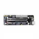
- The product functions as an Oculink-to-PCIe adapter, supporting PCIe 4.0 x4 speeds of up to 64 Gbps.
- This product is part of the Female PCBA series, an Oculink graphics card dock motherboard development board.
- The Oculink female connector is SFF8612, and the Oculink male connector is SFF8611.
- Supports synchronized startup with the host or can be manually powered on via a switch cable. Use a full-function Oculink data cable; OC1A-50CM is recommended.
- Does not support hot-swapping—no insertion or removal of components while powered on.
CoWoS is TSMC’s 2.5D packaging technology family. It brings multiple dies together using an interposer-based package, creating a short, dense path for communication between dies; CoWoS packages can also integrate high-bandwidth memory. TSMC describes CoWoS as part of its 3DFabric portfolio. The PHY is not itself a packaging technology: it is the interface circuitry implemented in a system that uses the package.
In its 2025 silicon announcement, GUC said its test chip used multiple dies with north-south and east-west IP orientations connected through a CoWoS interposer. That points to package-level topology as part of the demonstration, not just an isolated PHY block. CoWoS also brings added design, assembly, power-delivery, thermal and test demands; the interconnect does not eliminate those costs or constraints.
What “32G” and 10 Tbps/mm mean
GUC’s “32G” means 32 gigabits per second per lane. It does not mean 32 gigabytes per second, and it is not the aggregate bandwidth of a complete package. In standards materials, physical rates are commonly expressed in gigatransfers per second (GT/s). Although GUC describes its figure in Gbps per lane, the encoding and protocol context matter, so the units should not be treated as interchangeable in every calculation.
Rank #3

- Support NVMe protocol and M.2 solid state drive protocol, high-speed read/write, with high work efficiency.
- PCI-E×1 only supports Gen2 or Gen3 mode.
- Only supports PI5B. Compatible with M.2 solid state drive of 2230/2242 sizes.
- Onboard working indicator lights, with PWR on continuously when powered, and ACT blinking during read/write.
- Integrate heat dissipation and M.2 expansion.
Total bandwidth depends on lane count, the number and direction of links, package topology and protocol overhead. A physical signaling rate is not the same as usable application payload: framing, flow control and other implementation overhead can reduce the data available to software or compute engines.
GUC’s 10 Tbps/mm figure is a bandwidth-density claim: an amount of interface bandwidth associated with a millimeter of die edge under the company’s design assumptions. The release also gives 5 Tbps/mm full-duplex. Neither number is total chip bandwidth, and neither should be generalized to every UCIe implementation without matching assumptions about lane placement, directions and measurement conventions. TSMC has separately reported a 32-Gb/s UCIe-compliant 3nm interface with 10.5 Tb/s/mm beachfront density and 0.6 pJ/b in a research presentation; that is separate TSMC data, not evidence that GUC’s design achieved those same results. TSMC’s presentation provides that separate context.
From tape-out to silicon
Tape-out means a design has been finalized and released for manufacturing. It is an important engineering milestone, but it does not by itself establish production yield, customer qualification, volume availability or commercial adoption. For this program, the public timeline has three distinct stages:
Rank #4

- 【Compatibility】The adapter board is specifically engineered to be compatible with the Raspberry Pi 5, leveraging its advanced features and connectivity options to deliver enhanced storage performance.
- 【NVMe SSD Supported】It allows for the connection of NVMe SSDs to the Raspberry Pi 5, enabling users to take advantage of the high-speed data transfer rates and low latency offered by NVMe technology.
- 【Plug-and-Play Installation】Designed for simplicity and convenience, the adapter board offers plug-and-play functionality, allowing users to quickly install and configure NVMe SSD storage without the need for complex setup procedures.
- 【M-key Slot Compatibility】The adapter board is designed to accommodate M.2 NVMe SSDs with M-key slots, ensuring a secure and stable connection between the SSD and the Raspberry Pi 5.
- 【Form Factor Support】The adapter board supports both the 2242 and 2230 form factors, referring to the dimensions of the SSD. This means it can accommodate SSDs that are either 22mm wide and 40mm long (2242) or 22mm wide and 30mm long (2230).
- November 2023: GUC later identified this as the design-finalization/tape-out period for its 3nm UCIe/32G design.
- January 10, 2024: GUC publicly announced the successful tape-out.
- March 13, 2025: GUC announced the successful launch of 32G UCIe silicon on TSMC N3P and CoWoS, describing the silicon as supporting UCIe 2.0 and 32 Gbps per lane.
The later announcement is meaningful progress beyond the tape-out claim, but it is not by itself evidence that a named customer product entered mass production. See GUC’s 2025 silicon announcement and its later corporate disclosure for the company’s reported milestones.
How it fits GUC’s later roadmap
The 32G N3P/CoWoS silicon is a UCIe 2.0-era milestone, not a UCIe 3.0 product by default. The UCIe Consortium announced UCIe 3.0 in August 2025, adding 48 GT/s and 64 GT/s rates to the specification’s data-rate family. GUC subsequently announced a separate face-up UCIe IP tape-out on TSMC N5 for SoIC-X, targeting 36 Gbps, in July 2025; that is distinct from the 3nm CoWoS design. In February 2026, GUC announced tape-out of UCIe 64G IP on N3P and CoWoS, associated with UCIe 3.0. These later developments show roadmap progression, not a change to what the January 2024 announcement covered. See the consortium’s releases, GUC’s N5/SoIC-X announcement and GUC’s 64G announcement.
The Tool Desk
Outbyte PC Repair FREEClear out junk files and repair common Windows errorsFree Scan →Outbyte Driver Updater FREEScan for outdated or missing drivers - takes under a minuteDriver Scan →What a customer would still have to evaluate
For a customer considering this class of IP, the reported rate is only one part of the decision. The implementation must fit the customer’s lane configuration, protocol needs, package rules, power budget and thermal envelope. Interoperability also requires system-level validation: matching protocol versions and configurations does not automatically guarantee that arbitrary chiplets will work together.
Best Value

- 75T FPGA DMA Card with XC7A75T Chip The D DICHEN 75T FPGA DMA card is built with an XC7A75T Artix-7 FPGA chip, offering strong logic density, signal processing capability, embedded memory support, LVDS I/O, and efficient power-to-performance balance for professional hardware workflows.
- USB-C and PCIe x1 Connectivity Designed with USB-C and PCIe x1 interfaces, this FPGA DMA board supports flexible connection options for desktop PC hardware projects, FPGA development, data acquisition, lab testing, and advanced electronics validation
- PCILeech Compatible Development Board This DMA card is compatible with PCILeech-related development workflows, making it suitable for authorized research, firmware testing, hardware debugging, and professional system validation. Users should operate it only in legal and permitted environments.
- Compact Hardware Design with Tutorial USB The compact board measures approximately 2.7 x 1.5 x 0.35 inches and includes a tutorial USB drive plus 2 USB-A cables, helping experienced users complete basic setup, connection, and configuration more efficiently.
- Built for Professional Hardware Projects Ideal for FPGA development, PCIe hardware testing, signal processing, embedded system experiments, and data-intensive electronics projects. This product is recommended for users with FPGA, PCIe, firmware, or computer hardware experience.
The announcement is specifically tied to TSMC N3P and CoWoS. A design using another foundry, process node, interposer, bump pitch or package flow could need a different IP implementation or supplier. CoWoS can enable high-density connections, but its package and assembly costs, capacity planning, power integrity, heat removal and test strategy remain important engineering and business constraints.
GUC presents its chiplet offering as broader than a standalone PHY, encompassing design support, package engineering, electrical and thermal simulation, DFT and production testing. That wider scope may matter to teams seeking support across integration, but the tape-out and silicon milestones alone do not establish the economics, availability or production readiness of any particular customer project.
Quick Recap
Product prices and availability are accurate as of the date/time indicated and are subject to change. Any price and availability information displayed on Amazon at the time of purchase will apply.
Free tools Windows power users keep installed
One-click scans. No signup required.

