Free tools Windows power users keep installed
One-click scans. No signup required.
Some links on this page are affiliate links: if you buy through them we may earn a commission, at no extra cost to you.
A conventional gallium-nitride (GaN) PIN photodiode converts ultraviolet light into current without multiplying the charge inside the detector. A GaN PIN avalanche photodiode (APD) uses impact ionization to multiply that current, which can help detect weak signals—but adds avalanche noise, high-voltage bias and tighter operating requirements. “PIN” describes the junction structure; “avalanche” describes how the detector operates, so a PIN APD is not a contradiction.
What do GaN, PIN and APD mean?
GaN describes the semiconductor
Gallium nitride is a wide-bandgap semiconductor used in ultraviolet (UV) detectors. Its material properties can support UV-selective response, but “GaN” alone does not specify a detector’s exact wavelength range or make it solar-blind. Response depends on the material composition and device structure, as well as the window and packaging. Aluminum gallium nitride (AlGaN) is often used to reach shorter UV wavelengths.
Substrate and material quality matter, too. GaN devices may be grown on substrates such as sapphire or silicon carbide; lattice and thermal-expansion mismatch can affect defects and device performance. A review of III-nitride UV detectors discusses these substrate-related challenges: UV photodetectors based on III-nitrides.
What’s actually slowing this PC down?
Pick the symptom - the matching free tool is one click away.
PIN describes a junction structure
A PIN photodiode has p-type and n-type regions separated by an intrinsic or lightly doped region. Light absorbed in the device generates electron-hole pairs, which the electric field collects as current. A conventional PIN photodiode has no intentional internal avalanche multiplication. It can still use reverse bias—within its ratings—to reduce junction capacitance or improve carrier collection.
#1 Best Overall

- Photosensitive surface diameter: 230um
- Response wavelength: 400-1100nm
- Dark current: 0.03nA@M=100
- Response time: 0.3ns @ 905nm
- Package: TO-46 Can with ball lens cap
“No internal gain” does not mean that the whole circuit has no gain: a transimpedance amplifier (TIA) can convert the detector current into a larger voltage.
APD describes an operating mechanism
An APD is reverse-biased to create a strong electric field. Photogenerated carriers gain enough energy to trigger impact ionization, producing additional carriers and multiplying the photocurrent. The gain is commonly represented by M and changes with bias; it rises as the device approaches breakdown. Hamamatsu’s APD overview describes this internal-gain principle.
PIN and APD are therefore not mutually exclusive labels: a PIN-like layer structure can be engineered to operate as an APD. Actual APD structures vary, and a useful one requires a designed electric-field profile and controlled multiplication—not simply more voltage applied to an ordinary PIN diode.
How do the two detectors compare?
| Characteristic | Conventional GaN PIN photodiode | GaN PIN APD |
|---|---|---|
| Internal multiplication | No intentional avalanche gain; photocurrent tracks absorbed light. | Impact ionization multiplies photocurrent by a bias-dependent gain. |
| Bias and readout | Zero or relatively low reverse bias, depending on the device; readout commonly uses a TIA. | High reverse bias near controlled breakdown; still requires readout electronics, plus careful bias management. |
| Weak-signal performance | Limited by photocurrent and the noise of the detector and readout. | Can help when the following amplifier’s input-referred noise is a major limitation; avalanche noise can reduce the benefit. |
| Noise | Can include shot, thermal, generation-recombination and amplifier noise. | Has those relevant noise sources plus avalanche excess noise, gain fluctuations and sensitivity to bias-supply noise. |
| Speed | Depends on transit time, capacitance, area and readout bandwidth. | Also depends on those factors; avalanche build-up can add delay. An APD is not automatically faster. |
| Linearity and temperature | Often simpler to operate predictably within the specified range; dark current and responsivity can still vary with temperature. | Gain and breakdown behavior can vary with voltage and temperature; check gain compression and the specified operating range. |
| System complexity | Typically simpler bias and protection requirements. | Usually needs a low-noise high-voltage supply, current limiting, monitoring and often temperature compensation. |
| Availability | Commercial GaN PIN products are listed by vendors. | The sources cited here establish research devices, but not a broadly available, publicly priced catalog GaN PIN APD. |
These are architectural tendencies, not guarantees for every part. Compare device specifications under equivalent wavelength, bias, temperature, optical-power and readout conditions.
Rank #2

- Photoelectric IV conversion module
- Power supply: 12V
- Dimensions: (PCB) 56mm* 43mm (positioning hole) 48mm * 35mm
- Signal input: receiving an avalanche photodiode to receive optical signals
- Avalanche photodiode bias voltage adjustment range: 70V~180V Bandwidth: 1KHz-150MHz (default configuration), DC-1KHz (customer needs to configure, change C21 to 0 ohm resistor) APD avalanche photodiode driver
When does avalanche gain improve a measurement?
Responsivity and multiplication
Responsivity is photocurrent divided by incident optical power:
R = Iphoto / Poptical
For an APD in linear avalanche mode, a simplified relationship is:
RAPD ≈ M Runity
Here, Runity is responsivity before avalanche multiplication, and M is the multiplication gain. A high A/W figure may reflect internal gain rather than unusually high intrinsic photon-to-carrier conversion. To interpret a specification, look for its wavelength, bias, temperature, optical power and whether the responsivity includes avalanche gain.
Gain does not erase noise
An APD’s internal gain can make the signal larger relative to noise contributed after the detector, especially the TIA’s input-referred noise. It does not create a free improvement in signal-to-noise ratio: avalanche multiplication adds excess noise, and detector shot noise and dark current still matter. Increasing gain can eventually make the result worse.
Rank #3
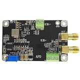
- APD Avalanche Photodiode Driver Photoelectric I-V Converter
A simplified APD shot-noise relationship is:
in2 = 2q(Idark + M Iphoto)F(M)B
where q is the elementary charge, B is bandwidth, and F(M) represents avalanche excess noise. This form is useful for showing the trade-off; real noise budgeting must also include the readout and operating conditions. Choose gain based on measured system noise, not the largest gain the device can reach.
Research results are not default specifications
Published GaN APDs demonstrate what particular structures can achieve, not what every device will deliver. A 2006 study reported stable optical gain above 1,000 near 360 nm in APDs grown on bulk GaN: the study’s reported results. A 2020 research device reported breakdown near 278 V, responsivity up to 60 A/W and gain of 105, with operation demonstrated up to 525 K: the device report. Those values are specific to the studies’ devices and test conditions; they are not general purchasing specifications.
What do bias and readout circuits require?
Conventional PIN circuit
A typical signal path is UV input → GaN PIN photodiode → optional reverse-bias source → TIA → filtering and an ADC or comparator. The TIA must suit the detector’s capacitance and expected photocurrent. Also account for ambient-light rejection, bias filtering, optical geometry and UV-window transmission.
The Tool Desk
Outbyte Driver Updater FREEFix the driver behind crashes, sound loss and screen glitchesFind Drivers →Outbyte PC Repair FREERepair Windows errors before they cause bigger problemsFix Now →APD circuit
An APD has the same basic optical and readout needs, but adds a high-voltage reverse-bias source, low-noise filtering, current limiting, bias monitoring and overvoltage protection. Gain may need calibration or temperature compensation. The TIA must handle the multiplied current and detector capacitance. Geiger-mode operation above breakdown additionally requires quenching and is a different operating mode from linear APD detection.
Rank #4

- 905nm Silicon 500um Avalanche Photodiode With TO46 Can 2mm Flat Window Cap
- Response wavelength: 400-1100nm
An APD does not eliminate the need for external readout. Its internal gain may reduce the external gain required, but the output still needs suitable electronics. Some commercial modules integrate an APD with high-voltage supply, amplification and temperature-compensation functions; see Hamamatsu’s APD module technical information.
Breakdown voltage is specific to a device and structure. Published GaN APD examples include approximately 48 V for a particular p-i-p-i-n design, approximately 90 V for some sapphire-based devices and approximately 278 V for a bulk-GaN device; these figures are not interchangeable. See the p-i-p-i-n study, the UV photodetector review and the 2020 device report. In linear mode, APDs normally operate below breakdown; avoid uncontrolled startup, voltage transients and operation beyond the manufacturer’s ratings.
Is a GaN APD faster or more sensitive than a GaN PIN?
Not by definition. Speed depends on carrier transit time, absorption-layer thickness, junction capacitance, active area, package parasitics, reverse bias, optical spot size and readout bandwidth. APDs also have avalanche build-up time. Compare rise time or bandwidth only when test conditions are stated and comparable.
PC Slower Than It Used to Be?
A free scan shows the junk files, broken settings and background clutter dragging Windows down - then fixes them in one click.Free scan · Windows 10 & 11Outdated Drivers Are Slowing You Down
One free scan finds every outdated or missing driver and matches the right update for your exact hardware.Free scan · exact hardware matchFor scale, Advanced Photonix lists a typical 1 ns rise and fall time for one GaN photodiode, model SD008-2151-012, with a 0.28 mm × 0.28 mm active area and 5 pF capacitance. Its datasheet lists a spectral range of 220–370 nm and responsivity of 0.18 A/W at 350 nm: model datasheet. These are specifications for that PIN device, not a comparison with an APD under matched conditions.
Best Value

- Full specifications are available at the Cremat website
- Equivalent noise charge (ENC): 200 electrons rms with input unconnected and with 1us shaping time.
- Gain: 1.4 volts per picocoulomb
- Unsaturated output swing: -3 volts to + 3 volts with unloaded output
Likewise, APD sensitivity depends on the whole system. If amplifier noise dominates, multiplication may help; if shot noise, dark current, avalanche excess noise or background light dominates, more gain may provide little benefit. A large-area PIN can also be slower than a small APD, while a high-gain APD may be slowed by its multiplication process.
Independent reader supportYour contribution helps us test, update, and keep practical guides available for everyone.How should you choose for a UV system?
Choose a GaN PIN photodiode when
- The signal is moderate or strong enough for a conventional TIA.
- Low-voltage operation, straightforward calibration and predictable linear behavior are priorities.
- You are building UV monitoring, spectroscopy, flame sensing, disinfection monitoring or industrial control, and the selected device covers the wavelength.
- High-voltage design and gain stabilization would add more complexity than useful signal.
Evaluate a GaN PIN APD when
- The UV signal is genuinely weak and the following amplifier’s input-referred noise is limiting detection.
- The system can accommodate high-voltage bias, protection, temperature management and characterization.
- You can obtain reliable device data for gain, excess noise, dark current, breakdown margin and operating conditions.
- The expected signal level does not saturate the multiplication region or readout.
Consider another detector family when
- Your wavelength falls outside the selected GaN device’s useful response; for near-infrared telecom wavelengths, InGaAs devices may be more appropriate.
- You require single-photon counting and a qualified SPAD, photomultiplier tube or related module better fits the system.
- You need an established catalog APD supply rather than a custom or research-stage GaN device. A silicon APD may be an alternative for some UV-to-visible applications, but verify its spectral response, packaging and environmental suitability.
- The system cannot safely generate and regulate the detector’s required reverse voltage.
What should you check on a datasheet?
Compare devices at the wavelength and operating conditions your system will actually use. Ask vendors or authors to state the following:
- Material and alloy composition, device structure and substrate.
- Illumination direction, active area, spectral-response curve and peak wavelength.
- Responsivity at the target wavelength, and whether an APD value is unity-gain or multiplied.
- For an APD: gain definition, operating bias, breakdown voltage, operating mode and gain-versus-bias behavior.
- Dark current at a stated bias and temperature; noise-equivalent power (NEP) and its measurement bandwidth.
- Detectivity, with the active area, bandwidth, wavelength and noise assumptions used to calculate it.
- Junction capacitance, rise time or bandwidth, including test conditions and load.
- Operating-temperature range, temperature coefficient and any compensation requirements.
- Optical power, spot size and calibration method used for reported measurements.
Useful relationships include IAPD = M Iprimary and D* = √(AΔf) / NEP, where A is detector area and Δf is bandwidth. Detectivity figures are not directly comparable unless area, bandwidth, wavelength, bias, temperature and noise definition are consistent.
Recommended Free Tools
Can you buy a GaN PIN APD?
The available vendor information establishes commercial GaN PIN photodiodes, including Advanced Photonix products covering UVC, UVB and UVA bands. Its product family lists examples with ranges of 210–280 nm, 220–320 nm and 220–370 nm: GaN photodiode product information. The cited material does not establish a broadly available, publicly priced catalog GaN PIN APD. Published research performance should therefore not be mistaken for a standard catalog offering.
For a commercial APD alternative, Hamamatsu lists silicon APDs, including the short-wavelength S17268-02 with a typical breakdown voltage of 160 V: S17268-02 product page. It is a silicon device, not a GaN substitute by default; check the spectral response and suitability for the particular UV application. Vendor product pages cited here do not provide public prices.
Quick Recap
Product prices and availability are accurate as of the date/time indicated and are subject to change. Any price and availability information displayed on Amazon at the time of purchase will apply.

