Quick wins for a faster PC:
Fix the driver behind crashes, sound loss and screen glitchesFind Drivers →Clear out junk files and repair common Windows errorsFree Scan →Some links on this page are affiliate links: if you buy through them we may earn a commission, at no extra cost to you.
Yes—but with an important qualification. Voltera’s V-One can print conductive patterns on both sides of a small prototype board. To connect those sides, you must drill holes and install rivets; the machine does not plate vias as a conventional PCB manufacturer does. It is best viewed as an in-house rapid-prototyping and assembly system, not a like-for-like replacement for standard copper PCBs.
What “two-layer” means on the V-One
A V-One two-sided board starts with a rigid substrate, typically FR1 or FR4. The machine prints silver-based conductive ink on one face, then on the other. Where a circuit must pass between faces, the user drills a hole and installs a conductive rivet. The rivet—not ink plated through the hole—makes the electrical connection.
That distinction matters. A conventional fabricated two-layer PCB usually has plated-through holes connecting its copper layers. The V-One workflow instead depends on drilling, alignment, rivet installation and continuity checks. A printed board may be useful and functional, but it is not automatically equivalent to a standard plated-through-hole board.
Voltera describes the V-One as a system for printing traces, drilling, dispensing solder paste and reflowing components. Its product information lists double-sided PCB capability and a print area of about 128 × 116 mm. Voltera V-One product page · Technical specifications
#1 Best Overall
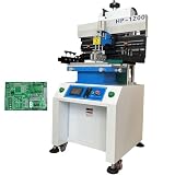
- Solder paste printing machine can be used in industrial electronics, automotive electronics, circuit components, mobile phone computer manufacturing and other industries. Touch screen key, automatic counting function, easy to use; Double suspension scraper and multi-function honeycomb aluminum alloy brush board make printing more flexible and reliable; Industrial PCL computer control, simple and convenient.
- Parameters: Positioning: PCB Outer Or Pin Positioning, Print-table size: 12.6"*27.7" (320*703mm), Max frame Size: 23.6"*31.5" (600*800mm), Substrate size: 16.7"*27.5" (500*700mm), Adjusting For Table: Front and back ±10mm, left and right ±10mm, Printing Accurary: ±0.02mm, Repeating Accurary: ±0.02mm, PCB Thickness: 0.2-2.0mm, Air Source: 4-6kg/cm2
- Scraper Holder. Precision guide rail and variable frequency motor drive knife holder conversion, high printing accuracy. Using unique program design, printing scraper seat adjustment is convenient; The front and rear block blades can be adjusted to select the appropriate printing position. The printing scraper can rotate up to 45 degrees and be fixed, making it easy to clean and replace the printing screen and scraper.
- The proofreading method adopts steel mesh movement, combined with printing (PCB) X, Y, Z. Calibration and fine-tuning are convenient and fast. High precision structure, using linear square track, with variable frequency motor drive, to ensure the stability and accuracy of printing base support.
- Breakthrough of printing effect: due to the different characteristics of red glue and solder paste, the machine's unique automatic setting of operating parameters can be suitable for different products to achieve good printing effect. The printing scraper can rotate up to 45 degrees and be fixed, making it easy to clean and replace the printing screen and scraper.
How a two-sided board is made
- Design for the process. Use V-One-compatible trace, spacing, hole and component clearances. The manufacturer’s guidelines list 0.2 mm (8 mil) as the minimum trace width and spacing, and recommend 10 mil for new users.
- Export Gerbers and drill data. The software accepts Gerber files and drill files. Common extensions identify top and bottom copper, solder-paste and drill layers. Check that the exported files correspond to the intended layers.
- Inspect the previews. Pay particular attention to the bottom layer: the software may automatically mirror bottom-layer files along the X axis. Compare the preview with the CAD layout and verify component orientation and drill locations before printing.
- Print and cure the first side. Secure the substrate, load the conductive-ink cartridge, print the first pattern and cure it according to Voltera’s procedure.
- Drill the required holes. The optional V-One Drill is used for vias and through-holes in the described workflow. A drilled hole alone does not make an electrical connection.
- Flip and register the board. The substrate must be aligned for the opposite-side print. Registration is manual, so careful positioning is part of the process.
- Print and cure the second side. Print the other conductive pattern, observing the same substrate and process requirements.
- Install the rivets and test. Set rivets in the designated holes, then use a multimeter to check each layer-to-layer connection and critical net before fitting components.
- Assemble if needed. The V-One can dispense solder paste and reflow components on its heated platform. Component placement is still a separate task, typically done by hand or with other equipment.
The exact sequence and software prompts can vary by design and software version; use the current V-One documentation and Voltera’s rivet instructions for the machine-specific procedure.
What the rivet connection does—and what to check
A rivet passes through the drilled substrate and is set so it makes contact with the conductive pads on both faces. It provides the through-board path where a conventional board would use a plated via. The pad geometry must leave enough overlap for the rivet and the print to meet; drilling or registration errors, a poorly set rivet, or contamination can leave an open connection.
Do not assume a via works because the rivet is physically present. Check continuity between the relevant top- and bottom-side pads, and check power, ground and other critical nets before assembly. The V-One does not automatically create or verify plated holes.
The Tool Desk
Outbyte PC Repair FREERepair Windows errors before they cause bigger problemsFix Now →Outbyte Driver Updater FREEScan for outdated or missing drivers - takes under a minuteDriver Scan →Rank #2

- 【Flexible Positioning】This solder paste printer adopts a universal honeycomb base plate, movable thimble, and movable support plate to position PCB flexibly, which can ensure convenient positioning.
- 【High Repetition Accuracy】The repeatability of this solder paste printer is ±0.01 mm. The circuit board is positioned with positioning pins, thimble, which is easy to position and can ensure the accuracy of repeated operations.
- 【Easy Calibration】The calibration can be achieved by moving the stencil and fine-tuning the X and Y axes of the printing platform for accurate alignment, which is convenient. The solder paste printer is fixed by a knob with a pressure plate, which is firm and stable.
- 【Adjustable Height】The stencil holder adopts a spiral screw bar, which can be adjusted up and down in height, making it easy to control the thickness of the PCB and the amount of printed solder paste.
- 【High-quality Material】The working platform is made of high quality aluminum plate with honeycomb positioning holes, and the bottom plate is made of thickened steel plate welded into shape, which is strong and durable.
Design limits to consider
| Design factor | Manufacturer guidance or specification | What it means in practice |
|---|---|---|
| Trace width and spacing | 0.2 mm (8 mil) minimum; 10 mil recommended for new users | Treat the minimum as a design guideline, not a guaranteed yield. More generous spacing is prudent when reliability matters or you are learning the process. |
| SMT component pitch | 0.65 mm minimum IC pin pitch in the general design guidelines; 0.5 mm cited for solder-paste printing | Check the specific print and assembly requirements for the package; these figures do not mean every board at that pitch will assemble successfully. |
| Passive components | 0603 listed as the general minimum; 0402 listed for solder-paste printing | Do not interpret 0402 paste support as a blanket guarantee for every 0402 layout or assembly. |
| Board area and thickness | About 128 × 116 mm print area; 1–3 mm substrate thickness | Large boards or substrates outside the specified range are not a fit for the stated workflow. |
| Layers and vias | Double-sided boards; drilled holes and rivets provide inter-layer connections | It is not a substitute for boards needing more than two layers or conventional plated-through holes. |
| Copper planes | Hatched planes recommended over solid planes | Follow the manufacturer’s layout guidance for large copper areas rather than assuming a solid pour will print like etched copper. |
| Positioning versus feature size | XYZ resolution listed as 10 × 10 × 1 µm; minimum trace width listed as 0.2 mm | Motion resolution is not the same as reliably printable electrical feature size. The 0.2 mm design rule is the relevant figure for trace planning. |
These figures come from Voltera’s V-One circuit-design guidelines and technical specifications. They are manufacturer guidance, not independent performance guarantees.
Printed silver ink is not ordinary copper
The V-One prints conductive silver-based ink, not copper foil. Voltera’s design documentation says the ink is approximately an order of magnitude less conductive than copper. As a result, a long, narrow printed trace can have more resistance and voltage drop than the equivalent copper trace.
For power rails, high-current paths, analog references and ground returns, assess the resistance and voltage drop of the actual printed geometry. Keep traces short and wide where the design allows, and validate temperature and circuit performance rather than assuming copper-board behavior. This material trade-off is one reason the V-One is a better fit for modest-current prototypes than demanding power distribution unless the design is specifically checked.
Rank #3
- ✔️【Flexible Positioning】This solder paste printer adopts a universal honeycomb base plate, movable thimble, and movable support plate to position PCB flexibly, which can ensure convenient positioning.The solder paste printer is fixed by a knob with a pressure plate, which is firm and stable.
- ✔️【High Repetition Accuracy】The repeatability of this solder paste printer is ±0.01 mm. The circuit board is positioned with positioning pins, thimble, which is easy to position and can ensure the accuracy of repeated operations.
- ✔️【Easy Calibration】The calibration can be achieved by moving the stencil and fine-tuning the X and Y axes of the printing platform for accurate alignment, which is convenient.
- ✔️【Adjustable Height】The stencil holder adopts a spiral screw bar, which can be adjusted up and down in height, making it easy to control the thickness of the PCB and the amount of printed solder paste.
- ✔️【High-quality Material】The working platform is made of high quality aluminum plate with honeycomb positioning holes, and the bottom plate is made of thickened steel plate welded into shape, which is strong and durable.The aluminum surface is corrosion resistant and easy to clean. You just need to wipe the dust with a damp rag.
Gerber handling and common failure points
The V-One software uses file extensions to identify intended layers. Voltera lists common top-copper extensions such as .gtl, .gbr, .top, .cmp and .art; bottom-copper extensions include .gbl, .bottom, .sol and .art. Solder-paste and drill files have their own recognized extensions, including .gtp, .gbp, .drl and .drill. Consult the current file and design guidance for the complete mapping.
- Bottom-layer orientation: Because bottom files may be mirrored automatically, inspect the preview against the design before printing.
- Via opens: A misaligned hole, insufficient pad overlap or poorly set rivet can interrupt the connection. Test continuity before assembly.
- Large solid pours: Voltera recommends hatched rather than solid planes. Follow that guidance and check the print preview.
- Ink or paste dispensing issues: Nozzle condition, loading and print settings affect results. The documentation includes troubleshooting for print quality, paste purging and nozzle problems.
- First-print delays: Setup, calibration, substrate preparation, alignment and troubleshooting can add time, particularly for a first attempt.
Voltera promotes making a functional prototype in roughly an hour or less, but that should not be read as a guaranteed end-to-end time for every two-sided board. Curing, flipping, manual registration, drilling, riveting, continuity testing, component placement, reflow, cooldown and rework all contribute to the actual schedule. See the first-print workflow.
Independent reader supportYour contribution helps us test, update, and keep practical guides available for everyone.Drill, assembly and safety
The drill is not included in the base configuration shown on Voltera’s product and store pages; it is sold separately or offered as a configuration choice. A buyer planning the two-sided rivet workflow should account for the drill attachment and compatible bits, along with ink, solder paste, nozzles, substrates, rivets and rivet-setting tools. The store listing shows configurations and current purchase details, which can change.
Rank #4
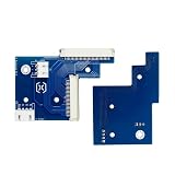
- This product has undergone rigorous testing and is manufactured from high-quality materials to meet your replacement needs.
- Reliable and durable.
- Please check your model number to ensure the product is compatible with your machine.
- Highly practical and easy to install.
- Highly reliable and perfectly matched to the originalequipment.
The V-One’s solder-paste dispenser and heated platform extend it beyond trace printing. Voltera specifies a 550 W heater reaching up to 240°C for as long as 60 minutes. Follow the solder-paste manufacturer’s thermal profile; reflowing a prototype is not the same as qualifying a production thermal process. The hot platform can burn, so use a suitable ventilated workspace and follow the V-One safety manual for hot surfaces, moving parts, sharp accessories, ink and solder-paste handling.
Who benefits from a V-One?
The V-One makes the most sense when iteration speed has real value: a lab that needs to test a revised circuit today, a startup protecting sensitive design files, or a university or makerspace sharing equipment among many users. It combines printing, drilling, paste dispensing and reflow in one workstation, and an in-house workflow can avoid waiting for an external order.
Recommended Free Tools
It is harder to justify for an individual who makes only occasional boards, a team whose design is already stable, or anyone focused on low-cost production. Voltera lists the base V-One at $3,499.99 USD before shipping and taxes, with the drill separate in the no-drill configuration. That is a capital purchase, not the complete ownership cost: consumables, accessories, operator time, maintenance and failed prints matter too. Check the current store price and configuration before budgeting.
A conventional board house is usually the more suitable route when a design needs standard copper, plated-through vias, solder mask, silkscreen, more than two layers, a larger board, or repeatable production quantities. For example, JLCPCB advertises prototype boards from $2 for five, though actual cost depends on dimensions, options and shipping. That is not an instant in-house alternative: ordering means supplier lead time and sending design files to an external service. Once a design is stable and assembled boards are needed, compare assembly quotations as well; JLCPCB’s assembly pricing information describes setup and other fee categories.
Before buying: a decision checklist
- Will same-day iteration save enough time or project cost to justify a dedicated machine?
- Are your boards within the approximately 128 × 116 mm print area and 1–3 mm substrate range?
- Can the circuit work with two printed sides and drilled, riveted connections?
- Can you design around silver ink’s higher resistance than copper?
- Do you need plated vias, solder mask, silkscreen, controlled-impedance RF features or more than two layers?
- Have you included the optional drill, consumables, substrates, rivets, maintenance and operator time in the budget?
- Do you have a suitable ventilated work area and the time to learn the calibration and maintenance workflow?
If conventional fabrication meets the project’s needs, ordering boards is likely the simpler and less capital-intensive choice. If the repeated cost of waiting, privacy concerns or the educational value of hands-on fabrication is substantial, the V-One may be worthwhile as a specialized prototyping tool.
Quick Recap
Product prices and availability are accurate as of the date/time indicated and are subject to change. Any price and availability information displayed on Amazon at the time of purchase will apply.
Free tools Windows power users keep installed
One-click scans. No signup required.

